
Datasheet


Table Of Contents
- FEATURES
- DESCRIPTION/ORDERING INFORMATION
- DESCRIPTION/ORDERING INFORMATION (CONTINUED)
- Absolute Maximum Ratings
- Recommended Operating Conditions
- Electrical Characteristics
- Switching Characteristics
- Switching Characteristics
- Switching Characteristics
- Switching Characteristics
- Switching Characteristics
- Operating Characteristics
- TYPICAL CHARACTERISTICS
- Typical Propagation Delay (A to B) vs Load CapacitanceTA = 25C, VCCA = 1.2 V
- Typical Propagation Delay (A to B) vs Load CapacitanceTA = 25C, VCCA = 1.5 V
- Typical Propagation Delay (A to B) vs Load CapacitanceTA = 25C, VCCA = 1.8 V
- Typical Propagation Delay (A to B) vs Load CapacitanceTA = 25C, VCCA = 2.5 V
- Typical Propagation Delay (A to B) vs Load CapacitanceTA = 25C, VCCA = 3.3 V
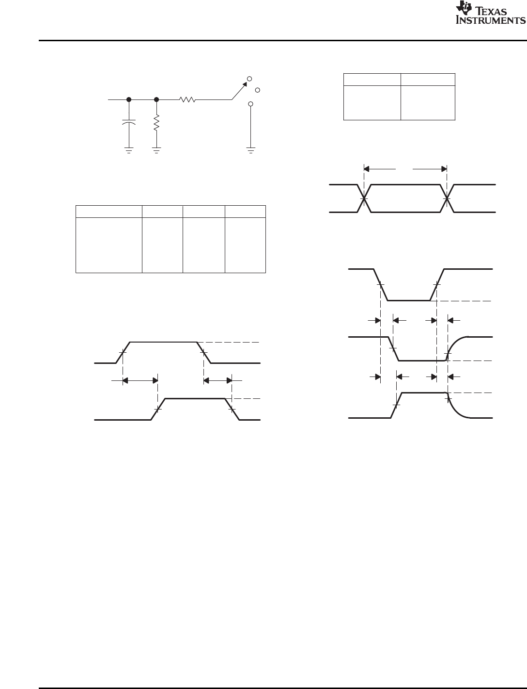
- PARAMETER MEASUREMENT INFORMATION
www.ti.com
PARAMETER MEASUREMENT INFORMATION
V
OH
V
OL
From Output
Under Test
C
L
(see Note A)
LOAD CIRCUIT
S1
2 × V
CCO
Open
GND
R
L
R
L
t
PLH
t
PHL
Output
Control
(low-level
enabling)
Output
Waveform 1
S1 at 2 × V
CCO
(see Note B)
Output
Waveform 2
S1 at GND
(see Note B)
t
PZL
t
PZH
t
PLZ
t
PHZ
V
CCA
/2V
CCA
/2
V
CCI
/2 V
CCI
/2
V
CCI
0 V
V
CCO
/2 V
CCO
/2
V
OH
V
OL
0 V
V
CCO
/2
V
OL
+ V
TP
V
CCO
/2
V
OH
− V
TP
0 V
V
CCI
0 V
V
CCI
/2 V
CCI
/2
t
w
Input
V
CCA
V
CCO
VOLTAGE WAVEFORMS
PROPAGATION DELAY TIMES
VOLTAGE WAVEFORMS
PULSE DURATION
VOLTAGE WAVEFORMS
ENABLE AND DISABLE TIMES
Output
Input
t
pd
t
PLZ
/t
PZL
t
PHZ
/t
PZH
Open
2 × V
CCO
GND
TEST S1
NOTES: A. C
L
includes probe and jig capacitance.
B. Waveform 1 is for an output with internal conditions such that the output is low, except when disabled by the output control.
Waveform 2 is for an output with internal conditions such that the output is high, except when disabled by the output control.
C. All input pulses are supplied by generators having the following characteristics: PRRv10 MHz, Z
O
= 50 Ω, dv/dt ≥ 1 V/ns.
D. The outputs are measured one at a time, with one transition per measurement.
E. t
PLZ
and t
PHZ
are the same as t
dis
.
F. t
PZL
and t
PZH
are the same as t
en
.
G. t
PLH
and t
PHL
are the same as t
pd
.
H. V
CCI
is the V
CC
associated with the input port.
I. V
CCO
is the V
CC
associated with the output port.
1.2 V
1.5 V ± 0.1 V
1.8 V ± 0.15 V
2.5 V ± 0.2 V
3.3 V ± 0.3 V
2 kΩ
2 kΩ
2 kΩ
2 kΩ
2 kΩ
V
CCO
R
L
0.1 V
0.1 V
0.15 V
0.15 V
0.3 V
V
TP
C
L
15 pF
15 pF
15 pF
15 pF
15 pF
SN74AVC8T245
8-BIT DUAL-SUPPLY BUS TRANSCEIVER
WITH CONFIGURABLE VOLTAGE TRANSLATION AND 3-STATE OUTPUTS
SCES517H – DECEMBER 2003 – REVISED FEBRUARY 2007
Figure 10. Load Circuit and Voltage Waveforms
12
Submit Documentation Feedback