
Datasheet
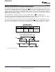
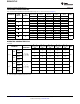
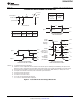


DIR1
A1
OE
B1
SN74AVC2T245
SCES692A –JUNE 2008–REVISED MAY 2012
www.ti.com
DESCRIPTION/ORDERING INFORMATION (CONTINUED)
The SN74AVC2T245 is designed for asynchronous communication between two data buses. The logic levels of
the direction-control (DIR) input and the output-enable (OE) activate either the B-port outputs or the A-port
outputs or place both output ports into the high-impedance mode . The device transmits data from the A bus to
the B bus when the B-port outputs are activated and from the B bus to the A bus when the A-port outputs are
activated. The input circuitry on both A and B ports always is active and must have a logic HIGH or LOW level
applied to prevent excess I
CC
and I
CCZ
.
The SN74AVC2T245 is designed so that the control pins (DIR1, DIR2, and OE) are supplied by V
CCA
.
This device is fully specified for partial-power-down applications using I
off
. The I
off
circuitry disables the outputs,
preventing damaging current backflow through the device when it is powered down.
The V
CC
isolation feature ensures that if either V
CC
input is at GND, both ports are in the high-impedance state.
To ensure the high-impedance state during power up or power down, OE must be connected to V
CC
through a
pull-up resistor; the minimum value of the resistor is determined by the current-sinking capability of the driver.
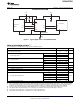
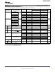
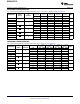
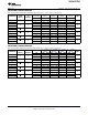
FUNCTION TABLE
(1)
(EACH TRANSCEIVER)
CONTROL INPUTS OUTPUT CIRCUITS
OPERATION
OE DIR1 A PORT B PORT
L L Enabled Hi-Z B data to A data
L H Hi-Z Enabled A data to B data
H X Hi-Z Hi-Z Isolation
(1) Input circuits of the data I/Os are always active.
LOGIC DIAGRAM (POSITIVE LOGIC)
(1) Shown for a single channel
2 Submit Documentation Feedback Copyright © 2008–2012, Texas Instruments Incorporated
Product Folder Link(s): SN74AVC2T245