
Datasheet
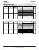

C
C
TG
C
C
TG
C
C
C
C
C
CLK
D
Q
C
TG
TG
SN74AUP2G79
SCES755C –DECEMBER 2009–REVISED JULY 2012
www.ti.com
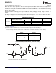
When data at the data (D) input meets the setup time requirement, the data is transferred to the Q output on the
positive-going edge of the clock pulse. Clock triggering occurs at a voltage level and is not directly related to the
rise time of the clock pulse. Following the hold-time interval, data at the D input can be changed without affecting
the levels at the outputs.
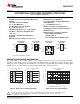
NanoStar™ package technology is a major breakthrough in IC packaging concepts, using the die as the
package.
This device is fully specified for partial-power-down applications using I
off
. The I
off
circuitry disables the outputs,
preventing damaging current backflow through the device when it is powered down.
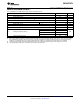
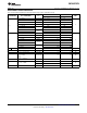
ORDERING INFORMATION
(1)
T
A
PACKAGE
(2)
ORDERABLE PART NUMBER TOP-SIDE MARKING
(3)
NanoStar™ – WCSP (DSBGA)
Reel of 3000 SN74AUP2G79YFPR _ _ H W _
0.23-mm Large Bump – YFP (Pb-free)
uQFN – DQE Reel of 5000 SN74AUP2G79DQER PT
–40°C to 85°C
QFN – RSE Reel of 5000 SN74AUP2G79RSER PT
SSOP – DCU Reel of 3000 SN74AUP2G79DCUR H79_
(1) For the most current package and ordering information, see the Package Option Addendum at the end of this document, or see the TI
web site at www.ti.com.
(2) Package drawings, thermal data, and symbolization are available at www.ti.com/packaging.
(3) DCU: The actual top-side marking has one additional character that designates the wafer fab/assembly site.
YFP: The actual top-side marking has three preceding characters to denote year, month, and sequence code, and one following
character to designate wafer fab/assembly site. Pin 1 identifier indicates solder-bump composition (1 = SnPb, • = Pb-free).
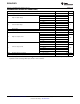
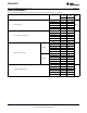
FUNCTION TABLE
INPUTS OUTPUT
CLK D Q
↑ H H
↑ L L
L X Q
0
H X Q
0
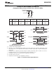
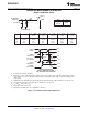
LOGIC DIAGRAM, EACH FLIP-FLOP (POSITIVE LOGIC)
Pin numbers shown are for the DCU and DQE packages.
2 Submit Documentation Feedback Copyright © 2009–2012, Texas Instruments Incorporated
Product Folder Link(s): SN74AUP2G79