
Datasheet

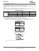


1
2 6
1Y
1OE
1A
7
5 3
2Y
2OE
2A
SN74AUP2G241
SCES761B –DECEMBER 2009–REVISED MAY 2010
www.ti.com
The SN74AUP2G241 is designed specifically to improve both the performance and density of 3-state
memory-address drivers, clock drivers, and bus-oriented receivers and transmitters.
NanoStar™ package technology is a major breakthrough in IC packaging concepts, using the die as the
package.
This device is fully specified for partial-power-down applications using I
off
. The I
off
circuitry disables the outputs,
preventing damaging current backflow through the device when it is powered down.
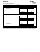
ORDERING INFORMATION
(1)
T
A
PACKAGE
(2)
ORDERABLE PART NUMBER TOP-SIDE MARKING
(3)
NanoStar™ – WCSP (DSBGA)
Reel of 3000 SN74AUP2G241YFPR _ _ H Q _
0.23-mm Large Bump – YFP (Pb-free)
uQFN – DQE Reel of 5000 SN74AUP2G241DQER HQ
–40°C to 85°C
QFN – RSE Reel of 5000 SN74AUP2G241RSER HQ
SSOP – DCU Reel of 3000 SN74AUP2G241DCUR H41_
(1) For the most current package and ordering information, see the Package Option Addendum at the end of this document, or see the TI
web site at www.ti.com.
(2) Package drawings, thermal data, and symbolization are available at www.ti.com/packaging.
(3) DCU: The actual top-side marking has one additional character that designates the wafer fab/assembly site.
YFP: The actual top-side marking has three preceding characters to denote year, month, and sequence code, and one following
character to designate the wafer fab/assembly site. Pin 1 identifier indicates solder-bump composition (1 = SnPb, ● = Pb-free).
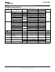
FUNCTION TABLES
INPUTS
OUTPUT
1Y
1OE 1A
L H H
L L L
H X Z
INPUTS
OUTPUT
2Y
2OE 2A
H H H
H L L
L X Z
LOGIC DIAGRAM (POSITIVE LOGIC)
Pin numbers shown are for DCU and DQE packages.
2 Submit Documentation Feedback Copyright © 2009–2010, Texas Instruments Incorporated
Product Folder Link(s): SN74AUP2G241