
Datasheet
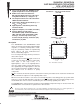


SN54ABT841, SN74ABT841A
10-BIT BUS-INTERFACE D-TYPE LATCHES
WITH 3-STATE OUTPUTS
SCBS196D – FEBRUARY 1991 – REVISED MAY 1997
4
POST OFFICE BOX 655303 • DALLAS, TEXAS 75265
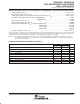
electrical characteristics over recommended operating free-air temperature range (unless
otherwise noted)
PARAMETER
TEST CONDITIONS
T
A
= 25°C SN54ABT841 SN74ABT841A
UNIT
PARAMETER
TEST
CONDITIONS
MIN TYP
†
MAX MIN MAX MIN MAX
UNIT
V
IK
V
CC
= 4.5 V, I
I
= –18 mA –1.2 –1.2 –1.2 V
V
CC
= 4.5 V, I
OH
= –3 mA 2.5 2.5 2.5
V
OH
V
CC
= 5 V, I
OH
= –3 mA 3 3 3
V
V
OH
V
CC
=45V
I
OH
= –24 mA 2 2
V
V
CC
=
4
.
5
V
I
OH
= –32 mA 2* 2
V
OL
V
CC
=45V
I
OL
= 48 mA 0.55 0.55
V
V
OL
V
CC
=
4
.
5
V
I
OL
= 64 mA 0.55* 0.55
V
V
hys
100 mV
I
I
V
CC
= 0 to 5.5 V, V
I
= V
CC
or GND ±1 ±1 ±1 µA
I
OZPU
‡
V
CC
= 0 to 2.1 V, V
O
= 0.5 V to 2.7 V, OE = X ±50 ±50 ±50 µA
I
OZPD
‡
V
CC
= 2.1 V to 0, V
O
= 0.5 V to 2.7 V, OE = X ±50 ±50 ±50 µA
I
OZH
V
CC
= 2.1 V to 5.5 V, V
O
= 2.7 V, OE ≥ 2 V 10 10 10 µA
I
OZL
V
CC
= 2.1 V to 5.5 V, V
O
= 0.5 V, OE ≥ 2 V –10 –10 –10 µA
I
off
V
CC
= 0, V
I
or V
O
≤ 4.5 V ±100 ±100 µA
I
CEX
V
CC
= 5.5 V, V
O
= 5.5 V Outputs high 50 50 50 µA
I
O
§
V
CC
= 5.5 V, V
O
= 2.5 V –50 –140 –180 –50 –180 –50 –180 mA
V55VI0
Outputs high 1** 250** 280 250 µA
I
CC
V
CC
= 5.5 V, I
O
= 0,
V
I
=V
CC
or GND
Outputs low 24** 38
¶
** 45
¶
38
¶
mA
V
I
=
V
CC
or
GND
Outputs disabled 0.5** 250** 280 250 µA
#
V
CC
=
5.5 V,
Outputs enabled 1.5 1.5 1.5 mA
∆I
CC
#
V
CC
=
5
.
5
V
,
One input at 3.4 V,
Outputs disabled 250** 280 250 µA
Other inputs at V
CC
or GND
Control inputs 1.5 1.5 1.5 mA
C
i
V
I
= 2.5 V or 0.5 V 4 pF
C
o
V
O
= 2.5 V or 0.5 V 7 pF
* On products compliant to MIL-PRF-38535, this parameter does not apply.
** These limits apply only to the SN74ABT841A.
†
All typical values are at V
CC
= 5 V.
‡
This parameter is characterized, but not production tested.
§
Not more than one output should be tested at a time, and the duration of the test should not exceed one second.
¶
This limit may vary among suppliers.
#
This is the increase in supply current for each input that is at the specified TTL voltage level rather than V
CC
or GND.
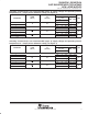
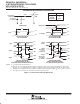
timing requirements over recommended ranges of supply voltage and operating free-air
temperature (unless otherwise noted) (see Figure 1)
V
CC
= 5 V,
T
A
= 25°C
SN54ABT841 SN74ABT841A
UNIT
MIN MAX MIN MAX MIN MAX
t
w
Pulse duration, LE high or low 3.3 3.3 3.3 ns
t
Setu
p
time data before LE↓
High 2.5 2.5 2.5
ns
t
su
Set
u
p
time
,
data
before
LE↓
Low 1.5 1.5 1.5
ns
t
h
Hold time data after LE↓
High 1.5 1.5 1.5
ns
t
h
Hold
time
,
data
after
LE↓
Low 1.5 2 1.5
ns