
Datasheet


SGLS128A − JULY 2002 − REVISED APRIL 2008
2
POST OFFICE BOX 655303 • DALLAS, TEXAS 75265
description (continued)
The SN65LVDM050Q and SN65LVDM051Q are characterized for operation from −40°C to 125°C. Additionally,
Q1 suffixed parts are qualified in accordance with AEC-Q100 stress test qualification for integrated circuits.
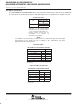
AVAILABLE OPTIONS
{
PACKAGE
}
T
A
SMALL OUTLINE
(D)
−40°C to 125°C
SN65LVDM050QDQ1
−40°C to 125°C
SN65LVDM051QDQ1
†
For the most current package and ordering
information, see the Package Option
Addendum at the end of this document, or
see the TI web site at http://www.ti.com.
‡
Package drawings, thermal data, and
symbolization are available at
http://www.ti.com/packaging.
NOTE:
The ultimate rate and distance of data transfer is dependent upon the attenuation
characteristics of the media, the noise coupling to the environment, and other
application-specific characteristics.
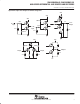
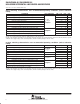
Function Tables
SN65LVDM050 and SN65LVDM051 RECEIVER
INPUTS OUTPUT
V
ID
= V
A
− V
B
RE R
V
ID
≥ 50 mV L H
−50 MV < V
ID
< 50 mV L ?
V
ID
≤ −50 mV L L
Open L H
X H Z
H = high level, L = low level, Z = high impedance,
X = don’t care
Function Tables (Continued)
SN65LVDM050 and SN65LVDM051 DRIVER
INPUTS
OUTPUTS
D DE Y Z
L H L H
H H H L
Open H L H
X L Z Z
H = high level, L = low level, Z = high impedance,
X = don’t care