
Datasheet


SGLS128A − JULY 2002 − REVISED APRIL 2008
17
POST OFFICE BOX 655303 • DALLAS, TEXAS 75265
APPLICATION INFORMATION
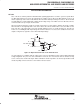
fail safe
One of the most common problems with differential signaling applications is how the system responds when
no differential voltage is present on the signal pair. The LVDS receiver is like most differential line receivers, in
that its output logic state can be indeterminate when the differential input voltage is between −50 mV and 50
mV and within its recommended input common-mode voltage range. TI’s LVDS receiver is different, however,
in how it handles the open-input circuit situation.
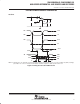
Open-circuit means that there is little or no input current to the receiver from the data line itself. This could be
when the driver is in a high-impedance state or the cable is disconnected. When this occurs, the LVDS receiver
pulls each line of the signal pair to near V
CC
through 300-kΩ resistors as shown in Figure 18. The fail-safe
feature uses an AND gate with input voltage thresholds at about 2.3 V to detect this condition and force the
output to a high-level, regardless of the differential input voltage.
Rt = 100 Ω (Typ)
300 kΩ 300 kΩ
V
CC
V
IT
≈ 2.3 V
A
B
Y
Figure 19. Open-Circuit Fail Safe of the LVDS Receiver
It is only under these conditions that the output of the receiver is valid with less than a 50-mV differential input
voltage magnitude. The presence of the termination resistor, Rt, does not affect the fail-safe function as long
as it is connected as shown in the figure. Other termination circuits may allow a dc current to ground that could
defeat the pullup currents from the receiver and the fail-safe feature.