
Car Stereo System - Car Radio Digital Signal Processor User Manual


www.ti.com
SM320C6455-EP
FIXED-POINT DIGITAL SIGNAL PROCESSOR
SPRS462B – SEPTEMBER 2007 – REVISED JANUARY 2008
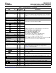
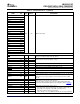
Table 2-3. Terminal Functions (continued)
SIGNAL
TYPE
(1)
IPD/IPU
(2)
DESCRIPTION
NAME NO.
AED21 AD29
AED20 AJ28
AED19 AF29
AED18 AH28
AED17 AE29
AED16 AG28
AED15 AF28
AED14 AH26
AED13 AE28
AED12 AE26
AED11 AD26
I/O/Z IPU EMIFA external data
AED10 AF27
AED9 AG27
AED8 AD27
AED7 AE25
AED6 AJ27
AED5 AJ26
AED4 AE27
AED3 AG25
AED2 AH27
AED1 AF25
AED0 AD25
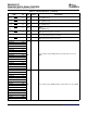
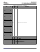
DDR2 MEMORY CONTROLLER (32 BIT) - CONTROL SIGNALS COMMON TO ALL TYPES OF MEMORY
DDR2 Memory Controller memory space enable. When the DDR2 Memory
DCE0 E14 O/Z
Controller is enabled, it always keeps this pin low.
DBA2 E15 O/Z
DBA1 D15 O/Z DDR2 Memory Controller bank address control
DBA0 C15 O/Z
DDR2CLKOUT B14 O/Z DDR2 Memory Controller output clock (CLKIN2 frequency × 10)
DDR2CLKOUT A14 O/Z Negative DDR2 Memory Controller output clock (CLKIN2 frequency × 10)
DSDCAS D13 O/Z DDR2 Memory Controller SDRAM column-address strobe
DSDRAS C13 O/Z DDR2 Memory Controller SDRAM row-address strobe
DSDWE B13 O/Z DDR2 Memory Controller SDRAM write-enable
DSDCKE D14 O/Z DDR2 Memory Controller SDRAM clock-enable (used for self-refresh mode)
DEODT1 A17 O/Z On-die termination signals to external DDR2 SDRAM. These pins should not be
connected to the DDR2 SDRAM.
Note: There are no on-die termination resistors implemented on the C6455
DEODT0 E16 O/Z
DSP die.
DSDDQGATE3 F21 I
DDR2 Memory Controller data strobe gate [3:0]
DSDDQGATE2 E21 O/Z
For hookup of these signals, please refer to the Implementing DDR2 PCB
DSDDQGATE1 B9 I
Layout on the TMS320C6455 application report (literature number SPRAAA7 ).
DSDDQGATE0 A9 O/Z
DSDDQM3 C23 O/Z DDR2 Memory Controller byte-enable controls
• Decoded from the low-order address bits. The number of address bits or
DSDDQM2 C20 O/Z
byte enables used depends on the width of external memory.
DSDDQM1 C8 O/Z
• Byte-write enables for most types of memory.
DSDDQM0 C11 O/Z
• Can be directly connected to SDRAM read and write mask signal (SDQM).
Submit Documentation Feedback Device Overview 37