
Car Stereo System - Car Radio Digital Signal Processor User Manual


Contents
SM320C6455-EP
FIXED-POINT DIGITAL SIGNAL PROCESSOR
SPRS462B – SEPTEMBER 2007 – REVISED JANUARY 2008
1 Features .............................................................................................................................. 7
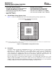
1.1 ZTZ/GTZ BGA Package (Bottom View) ................................................................................... 8
1.2 Description .................................................................................................................... 8
1.3 Functional Block Diagram ................................................................................................. 10
2 Device Overview ................................................................................................................. 11
2.1 Device Characteristics ..................................................................................................... 11
2.2 CPU (DSP Core) Description ............................................................................................. 12
2.3 Memory Map Summary .................................................................................................... 15
2.4 Boot Sequence ............................................................................................................. 17
2.4.1 Boot Modes Supported ......................................................................................... 17
2.4.2 2nd-Level Bootloaders .......................................................................................... 19
2.5 Pin Assignments ............................................................................................................ 20
2.5.1 Pin Map ........................................................................................................... 20
2.6 Signal Groups Description ................................................................................................ 24
2.7 Terminal Functions ......................................................................................................... 30
2.8 Development ................................................................................................................ 55
2.8.1 Development Support ........................................................................................... 55
2.8.2 Device Support .................................................................................................. 55
2.8.2.1 Device and Development-Support Tool Nomenclature ........................................ 55
2.8.2.2 Documentation Support ............................................................................. 56
3 Device Configuration .......................................................................................................... 59
3.1 Device Configuration at Device Reset ................................................................................... 59
3.2 Peripheral Configuration at Device Reset ............................................................................... 61
3.3 Peripheral Selection After Device Reset ................................................................................ 63
3.4 Device State Control Registers ........................................................................................... 65
3.4.1 Peripheral Lock Register Description ......................................................................... 66
3.4.2 Peripheral Configuration Register 0 Description ............................................................ 67
3.4.3 Peripheral Configuration Register 1 Description ............................................................ 69
3.4.4 Peripheral Status Registers Description ...................................................................... 70
3.4.5 EMAC Configuration Register (EMACCFG) Description ................................................... 73
3.4.6 Emulator Buffer Powerdown Register (EMUBUFPD) Description ........................................ 74
3.5 Device Status Register Description ...................................................................................... 75
3.6 JTAG ID (JTAGID) Register Description ................................................................................ 77
3.7 Pullup/Pulldown Resistors ................................................................................................. 78
3.8 Configuration Examples ................................................................................................... 78
4 System Interconnect ........................................................................................................... 81
4.1 Internal Buses, Bridges, and Switch Fabrics ........................................................................... 81
4.2 Data Switch Fabric Connections ......................................................................................... 82
4.3 Configuration Switch Fabric ............................................................................................... 84
4.4 Bus Priorities ................................................................................................................ 86
5 C64x+ Megamodule ............................................................................................................ 87
5.1 Memory Architecture ....................................................................................................... 87
5.2 Memory Protection ......................................................................................................... 90
5.3 Bandwidth Management ................................................................................................... 90
5.4 Power-Down Control ....................................................................................................... 91
5.5 Megamodule Resets ....................................................................................................... 91
5.6 Megamodule Revision ..................................................................................................... 92
5.7 C64x+ Megamodule Register Description(s) ........................................................................... 93
6 Device Operating Conditions ............................................................................................. 101
6.1 Absolute Maximum Ratings Over Operating Case Temperature Range (Unless Otherwise Noted) .......... 101
Contents 3