
Car Stereo System - Car Radio Digital Signal Processor User Manual


www.ti.com
7.7.3.8 PLL Controller Clock Align Control Register
SM320C6455-EP
FIXED-POINT DIGITAL SIGNAL PROCESSOR
SPRS462B – SEPTEMBER 2007 – REVISED JANUARY 2008
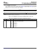
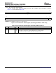
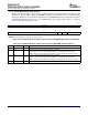
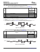
The PLL controller clock align control register (ALNCTL) is shown in Figure 7-18 and described in
Table 7-26 .
31 16
Reserved
R-0
15 5 4 3 2 0
Reserved ALN5 ALN4 Reserved
R-0 R-1 R-1 R-1
LEGEND: R/W = Read/Write; R = Read only; - n = value after reset
Figure 7-18. PLL Controller Clock Align Control Register (ALNCTL) [Hex Address: 029A 0140]
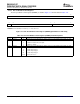
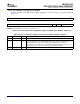
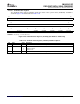
Table 7-26. PLL Controller Clock Align Control Register (ALNCTL) Field Descriptions
Bit Field Value Description
31:5 Reserved 0 Reserved. The reserved bit location is always read as 0. A value written to this field has no effect.
4:3 ALN n SYSCLK n alignment. Do not change the default values of these fields.
0 Do not align SYSCLK n to other SYSCLKs during GO operation. If SYS n in DCHANGE is set to 1,
SYSCLK n switches to the new ratio immediately after the GOSET bit in PLLCMD is set.
1 Align SYSCLK n to other SYSCLKs selected in ALNCTL when the GOSET bit in PLLCMD is set.
The SYSCLK n ratio is set to the ratio programmed in the RATIO bit in PLLDIV n.
2:0 Reserved 0 Reserved. The reserved bit location is always read as 0. A value written to this field has no effect.
Submit Documentation Feedback C64x+ Peripheral Information and Electrical Specifications 147