
Car Stereo System - Car Radio Digital Signal Processor User Manual

www.ti.com
7.7.3 PLL1 Controller Register Descriptions
7.7.3.1 PLL1 Control Register
SM320C6455-EP
FIXED-POINT DIGITAL SIGNAL PROCESSOR
SPRS462B – SEPTEMBER 2007 – REVISED JANUARY 2008
This section provides a description of the PLL1 controller registers. For details on the operation of the PLL
controller module, see the TMS320C645x DSP Software-Programmable Phase-Locked Loop (PLL)
Controller User's Guide (literature number SPRUE56 ).
NOTE: The PLL1 controller registers can only be accessed using the CPU or the emulator.
Not all of the registers documented in the TMS320C645x DSP Software-Programmable Phase-Locked
Loop (PLL) Controller User's Guide (literature number SPRUE56 ) are supported on the C6455. Only those
registers documented in this section are supported. Furthermore, only the bits within the registers
described here are supported. You should not write to any reserved memory location or change the value
of reserved bits.
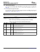
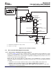
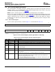
The PLL control register (PLLCTL) is shown in Figure 7-11 and described in Table 7-19 .
31 16
Reserved
R-0
15 8 7 6 5 4 3 2 1 0
PLL
Reserved Rsvd Rsvd Reserved PLLRST Rsvd PLLEN
PWRDN
R-0 R/W-0 R-1 R/W-0 R/W-1 R-0 R/W-0 R/W-0
LEGEND: R/W = Read/Write; R = Read only; - n = value after reset
Figure 7-11. PLL1 Control Register (PLLCTL) [Hex Address: 029A 0100]
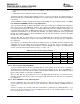
Table 7-19. PLL1 Control Register (PLLCTL) Field Descriptions
Bit Field Value Description
31:8 Reserved Reserved. The reserved bit location is always read as 0. A value written to this field has no effect.
7 Reserved Reserved. Writes to this register must keep this bit as 0.
6 Reserved Reserved. The reserved bit location is always read as 1. A value written to this field has no effect.
5:4 Reserved Reserved. Writes to this register must keep this bit as 0.
3 PLLRST PLL reset bit
0 PLL reset is released
1 PLL reset is asserted
2 Reserved Reserved. The reserved bit location is always read as 0. A value written to this field has no effect.
1 PLLPWRDN PLL power-down mode select bit
0 PLL is operational
1 PLL is placed in power-down state, i.e., all analog circuitry in the PLL is turned-off
0 PLLEN PLL enable bit
0 Bypass mode. Divider PREDIV and PLL are bypassed. All the system clocks (SYSCLK n) are
divided down directly from input reference clock.
1 PLL mode. Divider PREDIV and PLL are not bypassed. PLL output path is enabled. All the system
clocks (SYSCLK n) are divided down from PLL output.
C64x+ Peripheral Information and Electrical Specifications140 Submit Documentation Feedback