
Datasheet


Table Of Contents
- FEATURES
- APPLICATIONS
- DESCRIPTION
- ABSOLUTE MAXIMUM RATINGS
- RECOMMENDED OPERATING CONDITIONS
- PACKAGE SPECIFICATIONS
- ELECTRICAL CHARACTERISTICS
- PIN ASSIGNMENT
- TYPICAL CHARACTERISTICS (5-V INPUT) The electrical characteristic data has been developed from actual products tested at 25°C. This data is considered typical for the converter. Applies to , , and . The temperature derating curves represent the conditions at which internal components are at or below the manufacturer's maximum operating temperatures. Derating limits apply to modules soldered directly to a 100-mm × 100-mm, double-sided PCB with 2-oz. copper. Applies to .
- TYPICAL CHARACTERISTICS (12-V INPUT) The electrical characteristic data has been developed from actual products tested at 25°C. This data is considered typical for the converter. Applies to , , and . The temperature derating curves represent the conditions at which internal components are at or below the manufacturer's maximum operating temperatures. Derating limits apply to modules soldered directly to a 100-mm × 100-mm, double-sided PCB with 2-oz. copper. Applies to .
- APPLICATION INFORMATION
- REVISION HISTORY
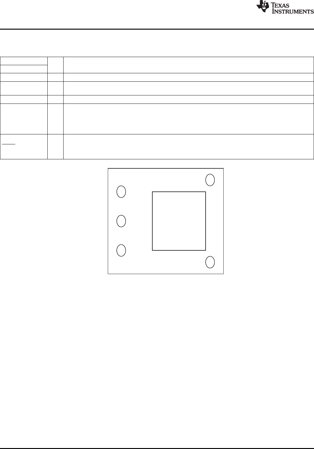
PIN
1
2
3
5
4
PTH08080W
SLTS235D –FEBRUARY 2005–REVISED SEPTEMBER 2013
www.ti.com
PIN ASSIGNMENT
TERMINAL FUNCTIONS
TERMINAL
I/O DESCRIPTION
NAME NO.
V
I
1 I The positive input voltage power node to the module, which is referenced to common GND.
This is the common ground connection for the V
I
and V
O
power connections. It is also the 0-Vdc reference for
GND 2
the Inhibit and V
O
Adjust control inputs.
V
O
3 O The regulated positive power output with respect to the GND node.
A 1% resistor must be connected between this pin and GND (pin 2) to set the output voltage of the module
higher than 0.9 V. If left open-circuit, the output voltage defaults to this value. The temperature stability of the
V
O
Adjust 4 I resistor should be 100 ppm/°C (or better). The set-point range is from 0.9 V to 5.5 V. The electrical
specification table gives the standard resistor value for a number of common output voltages. See the
application information for further guidance.
The Inhibit pin is an open-collector/drain-negative logic input that is referenced to GND. Applying a low-level
ground signal to this input disables the module's output. When the Inhibit control is active, the input current
Inhibit 5 I
drawn by the regulator is significantly reduced. If the Inhibit pin is left open-circuit, the module produces an
output voltage whenever a valid input source is applied. Do not place an external pull-up on this pin.
Figure 1. Terminal Location
TYPICAL CHARACTERISTICS (5-V INPUT)
(1) (2)
(1) The electrical characteristic data has been developed from actual products tested at 25°C. This data is considered typical for the
converter. Applies to Figure 2, Figure 3, and Figure 4.
(2) The temperature derating curves represent the conditions at which internal components are at or below the manufacturer's maximum
operating temperatures. Derating limits apply to modules soldered directly to a 100-mm × 100-mm, double-sided PCB with 2-oz. copper.
Applies to Figure 5.
4 Submit Documentation Feedback Copyright © 2005–2013, Texas Instruments Incorporated
Product Folder Links :PTH08080W