
Datasheet


Table Of Contents
- FEATURES
- APPLICATIONS
- DESCRIPTION
- ABSOLUTE MAXIMUM RATINGS
- RECOMMENDED OPERATING CONDITIONS
- ELECTRICAL CHARACTERISTICS
- DEVICE INFORMATION
- TYPICAL PERFORMANCE CURVES OF INTERNAL FILTER
- TYPICAL PERFORMANCE CURVES
www.ti.com
Microphone Amplifier
Input PGA
Sidetone Programmable Attenuator
Output Programmable Attenuator
V
COM1
and V
CCM2
Filter Pins
DAC
V
COM
10kW
20kW
FR/FL
C
f
SideTone
–
+
20kW
10kW
PCM2912
SLES216 – FEBRUARY 2008
The PCM2912 has the low-noise, single-ended mono microphone amplifier with mute function which is controlled
by MUTE (pin 30). The signal gain is selectable by MAMP (pin 23). The noise level at input node is 5 µ Vrms, and
the input impedance is 20 k Ω .
The PCM2912 has the low-noise input programmable gain amplifier (PGA) for the microphone amplifier
output/ADC input, whose gain range is +30 dB to – 12 dB in 1dB/step.
The PCM2912 has the low-noise, sidetone programmable attenuator with mute function for the sidetone signal
path (microphone amplifier output to output PGA input), whose gain range is 0 dB to – 76 dB in 1 dB/step.
The PCM2912 has the low-noise output programmable attenuator with mute function for mixed signal, which
affects DAC output signal and sidetone signal. The output PGA gain range is 0 dB to – 76 dB in 1 dB/step.
V
COM2
(pin 12) is provided for the center voltage of a headphone amplifier. V
COM1
(pin 11) is provided for the
center voltage of all other analog circuit. Each V
COM
pin must be decoupled with an appropriate capacitor.
Because the headphone output is disconnected when entering the suspend state, determining the capacitance is
important to prevent the pop-noise, especially for the V
COM2
(pin 12). The equivalent resistance of V
COM2
is 500
k Ω , and V
COM1
is 15 k Ω .
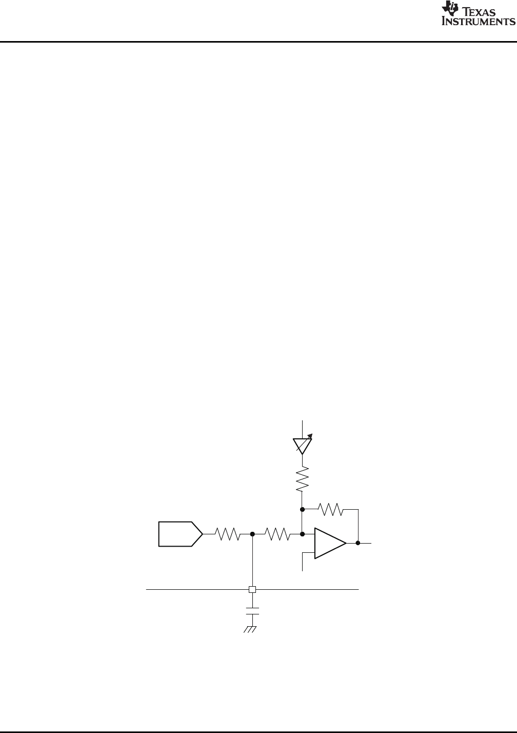
FL (pin 9) and FR (pin 10) are provided to make an LPF to decrease the DAC outband noise.
This is optional.
Figure 32. Filter Circuit
22 Submit Documentation Feedback Copyright © 2008, Texas Instruments Incorporated
Product Folder Link(s): PCM2912