
Datasheet


Table Of Contents
- FEATURES
- APPLICATIONS
- DESCRIPTION
- ABSOLUTE MAXIMUM RATINGS
- RECOMMENDED OPERATING CONDITIONS
- ELECTRICAL CHARACTERISTICS
- PIN ASSIGNMENTS
- TYPICAL CHARACTERISTICS: INTERNAL FILTER
- TYPICAL CHARACTERISTICS
- GENERAL DESCRIPTION
Endpoints
Internal Regulator
Clock and Reset
DAC
ADC
Microphone Bias
PCM2912A
www.ti.com
.......................................................................................................................................................................................... SLES230 – SEPTEMBER 2008
The PCM2912A has the following three endpoints:
• Control endpoint (EP #0)
• Isochronous out audio data stream endpoint (EP #1)
• Isochronous in audio data stream endpoint (EP #2)
The control endpoint is the default endpoint. The control endpoint controls all functions of the PCM2912A by the
standard USB request and USB audio class-specific request from the host. The isochronous out audio data
stream endpoint is an audio sink endpoint, which receives the PCM audio data. The isochronous out audio data
stream endpoint accepts the asynchronous transfer mode. The isochronous in audio data stream endpoint is an
audio source endpoint, which transmits the PCM audio data. The isochronous in audio data stream endpoint
uses synchronous transfer mode.
All required power sources are generated by five internal regulators.
Each regulator generates 3.3 V (typical, without load) from V
BUS
(pin 2). Each regulator has an output pin and a
ground return pin (as described in Table 6 ); this pair must be decoupled with an appropriate capacitor. Note that
this capacitance affects inrush-current limitation. One band-gap reference circuit supplies reference voltage for all
regulators. BGND (pin 1) is provided for reference ground of the band-gap reference.
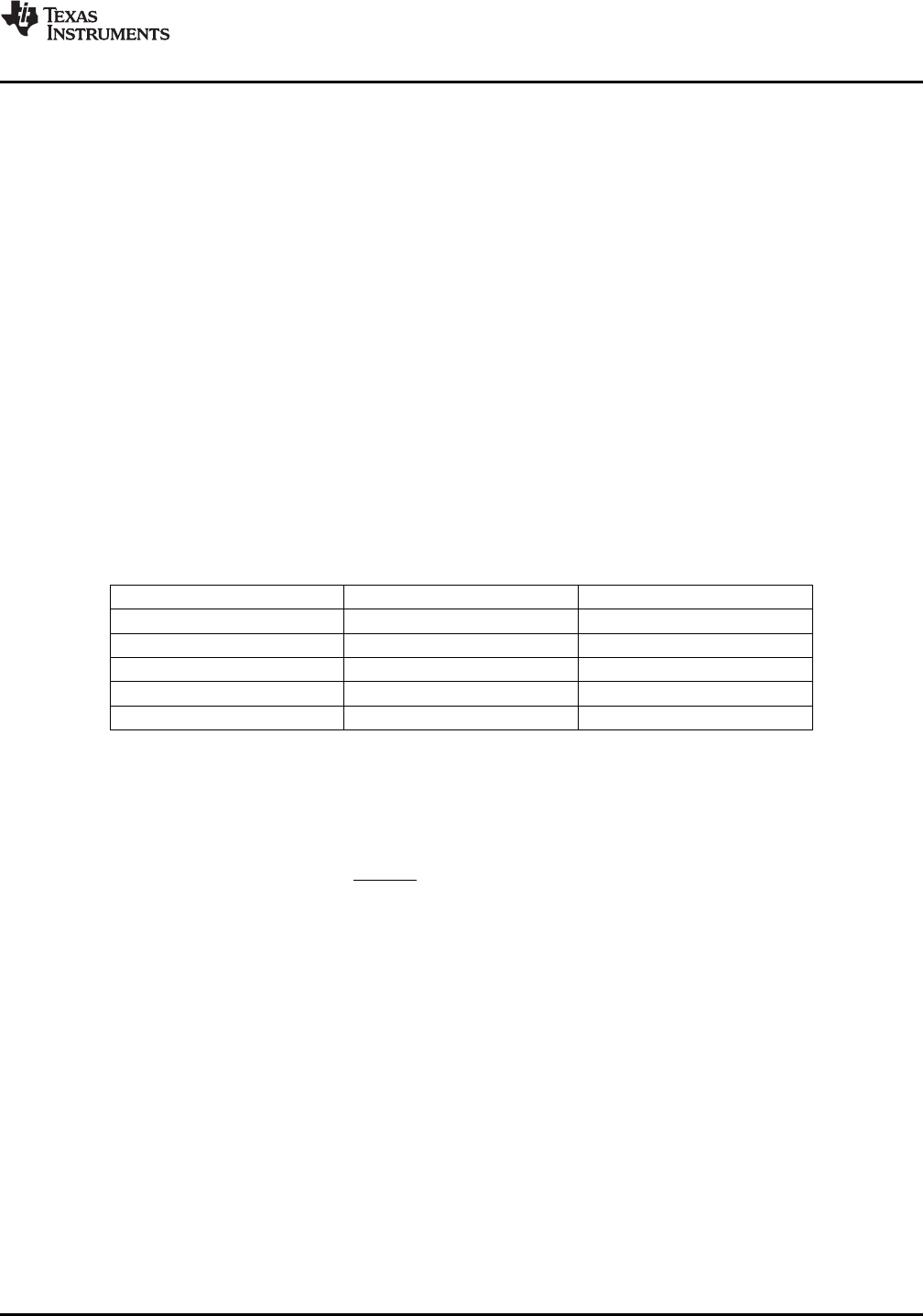
Table 6. Internal Regulator Summary
SUPPLIED CIRCUIT OUTPUT RETURN
Digital V
DD
(pin 5) DGND (pin 6)
Analog V
CCA
(pin 15) AGND (pin 13)
Headphone (L-ch) V
CCL
(pin 19) HGND (pin 20)
Headphone (R-ch) V
CCR
(pin 21) HGND (pin 20)
PLL V
CCP
(pin 26) PGND (pin 25)
The PCM2912A requires a 6-MHz ( ± 500 ppm) clock for USB function and audio function, which can be
generated from a built-in crystal oscillator with a 6-MHz crystal resonator. The 6-MHz crystal resonator must be
connected to XTI (pin 8) and XTO (pin 7) with one high (1-M Ω ) resistor and two small capacitors, whose
capacitance depends on the load capacitance of the crystal resonator. An external clock can be supplied through
XTI; if an external clock is supplied, XTO must be left open. Because there is no clock disabling signal, using the
external clock supply is not recommended. SSPND (pin 29) is unable to use clock disabling.
The PCM2912A has an internal power-on-reset circuit, which works automatically when V
BUS
(pin 2) exceeds 2.5
V, typical (2.2 V to 2.7 V), and approximately 700 µ s is required until the internal reset is released.
The PCM2912A has a stereo delta-sigma DAC that uses a 64-f
S
oversampling technique with an 8-f
S
oversampling digital filter. DAC outputs are provided through the headphone amplifier; V
OUT
L (pin 18) and V
OUT
R
(pin 22) provide 13 mW at 32 Ω and 0.6 V
CC
L/V
CC
R V
PP
at a 10-k Ω load.
The PCM2912A has a mono delta-sigma ADC that uses a 64-f
S
oversampling technique with a 1/64-f
S
decimation digital filter. The microphone input, V
IN
(pin 16), is fed to the ADC through a +20-dB microphone
amplifier and the PGA, which has +30 dB to – 12 dB in 1-dB steps.
The PCM2912A has a microphone bias generator, which provides a low-noise, 0.75-V
CCA
, 2-mA source current
output with appropriate output impedance for electret-microphone driving. This output, MBIAS (pin 17), should be
bypassed to AGND (pin 13) through an appropriate capacitor to reduce the output noise level.
Copyright © 2008, Texas Instruments Incorporated Submit Documentation Feedback 21
Product Folder Link(s): PCM2912A