
Datasheet


OPA567
SBOS287A
3
www.ti.com
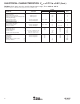
ELECTRICAL CHARACTERISTICS: V
S
= +2.7V to +5.5V
Boldface limits apply over the specified temperature range, T
A
= –40°C to +85°C.
At T
CASE
= +25°C, R
L
= 1kΩ, and connected to V
S
/2, unless otherwise noted.
NOTES:
(1) See typical characteristic,
Maximum Output Voltage vs Frequency
.
(2) See typical characteristic,
Total Harmonic Distortion + Noise vs Frequency
.
(3) Swing to the rail is measured in final test. Under those conditions, the A
OL
is derived from characterization.
(4) See Safe Operating Area (SOA) plots.
(5) See typical characteristic,
Overshoot vs Load Capacitance
.
(6) See the
Typical Characteristics
section. Higher frequency output impedance can affect frequency stability.
(7) External current limit setting resistor is required; see Figure 1.
(8) I
LIMIT
is the value of the desired current limit and is equal to 9800(I
SET
), where I
SET
is the current through the I
SET
pin. I
LIMIT
tolerance is proportional to the ratio of
I
LIMIT
/I
SET
. Errors from this parameter can be calibrated out—see the
Applications Information
section.
(9) V
SET
is a voltage reference that equals the difference between the voltage of the I
SET
pin and V–, and is referenced to the negative rail. Errors from this parameter
can be calibrated out—see the
Applications Information
section.
OPA567
PARAMETER CONDITION MIN TYP MAX UNITS
OFFSET VOLTAGE
Input Offset Voltage V
OS
I
O
= 0V, V
S
= +5V ±0.5 ±2mV
vs Temperature dV
OS
/dT T
A
= –40°C to +85°C ±1.3 µV/°C
vs Power Supply PSRR V
S
= +2.7V to +5.5V, V
CM
= (V–) +0.55V 12 60 µV/V
INPUT BIAS CURRENT
Input Bias Current I
B
±1 ±10 pA
vs Temperature (doubles every 10
°C)
Input Offset Current I
OS
±2 ±10 pA
NOISE
Input Voltage Noise Density, f = 1kHz e
n
12 nV/√Hz
f = 0.1Hz to 10Hz 8 µV
PP
Current Noise Density, f = 1kHz i
n
0.6 fA/√Hz
INPUT VOLTAGE RANGE
Common-Mode Voltage Range V
CM
Linear Operation (V–) – 0.1 (V+) + 0.1 V
Common-Mode Rejection Ratio CMRR V
S
= +5V, –0.1V < V
CM
< 3.2V 80 100 dB
V
S
= +5V, –0.1V < V
CM
< 5.1V 60 80 dB
INPUT IMPEDANCE
Differential 10
13
|| 4.5 Ω || pF
Common-Mode 10
13
|| 9 Ω || pF
OPEN-LOOP GAIN
Open-Loop Voltage Gain A
OL
0.2V
< V
O
< 4.8V, R
L
= 1kΩ, V
S
= +5V 100 126 dB
0.3V
< V
O
< 4.7V, R
L
= 1.15Ω, V
S
= +5V 90 dB
FREQUENCY RESPONSE
Gain Bandwidth Product GBW 1.2 MHz
Slew Rate SR G = +1, V
O
= 4.0V Step 1.2 V/µs
Full-Power Bandwidth
(1)
See Typical Characteristics
Settling Time: ±0.1% G = –1, V
O
= 4.0V Step 5 µs
Total Harmonic Distortion + Noise
(2)
THD+N See Typical Characteristics
OUTPUT
Voltage Output Swing from Rail V
O
R
L
= 1kΩ, A
OL
> 100dB (V–) + 0.2 (V
S
) ± 0.02 (V+) – 0.2 V
I
O
= ±2A, V
S
= +5V, A
OL
> 80dB
(3)
(V–) + 0.3 (V
S
) ± 0.2 (V+) – 0.3 V
Maximum Continuous Current Output: dc
(4)
2.4 A
Capacitive Load Drive
(5)
C
LOAD
See Typical Characteristics
Closed-Loop Output Impedance
(6)
R
O
G = 1, dc 0.1 Ω
G = 1, f = 10kHz 0.44 Ω
G = 1, f = 1.2MHz 45 Ω
Output Disabled Output Impedance 12M || 570 Ω || pF
CURRENT LIMIT (I
SET
Pin)
Output Current Limit
(7)
Externally Adjustable ±0.2 to ±2.2 A
Current Limit Equation
(8)
I
LIMIT
= I
SET
• 9800 A
R
SET
Equation R
SET
= 9800 (1.18V/I
LIMIT
) Ω
Current Limit Tolerance
(8)
, Positive I
LIMIT
= 1A ±3 ±10 %
Negative I
LIMIT
= 1A ±3 ±15 %
V
SET
Tolerance
(9)
(V–) + 1.05 (V–) + 1.18 (V–) + 1.3 V
ENABLE/SHUTDOWN INPUT
Enable Pin Bias Current V
SD
= 0V 0.2 µA
HIGH (Output enabled) V
SD
Pin Open or Forced HIGH (V–) + 2.5 V
LOW (Output disabled) V
SD
Pin Forced LOW (V–) + 0.8 V
Output Disable Time R
L
= 1Ω 0.5 µs
Output Enable Time R
L
= 1Ω 15 µs