
Datasheet


OPA567
SBOS287A
2
www.ti.com
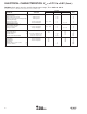
PIN # NAME DESCRIPTION
1, 12 V+ Positive Power-Supply Voltage
2, 3 V
O
Output
4, 5 V– Negative Power-Supply Voltage
6I
SET
Current Limit Set Pin
(1)
7I
FLAG
Current Limit Flag—Indicates when part is in
current limit (active LOW).
8 –IN Inverting Input
9 +IN Noninverting Input
10 T
FLAG
Thermal Flag—Indicates thermal stress (active
LOW).
11 ENABLE Enabled HIGH, shut down LOW.
ELECTROSTATIC
DISCHARGE SENSITIVITY
This integrated circuit can be damaged by ESD. Texas
Instruments recommends that all integrated circuits be handled
with appropriate precautions. Failure to observe proper han-
dling and installation procedures can cause damage.
ESD damage can range from subtle performance degrada-
tion to complete device failure. Precision integrated circuits
may be more susceptible to damage because very small
parametric changes could cause the device not to meet its
published specifications.
Supply Voltage ................................................................................. +7.5V
Output Current ............................................................... See SOA Curves
Signal Input Terminals (pins 8 and 9):
Voltage
(2)
............................................... (V–) – 0.5V to (V+) + 0.5V
Current
(2)
................................................................................ ±10mA
Output Short-Circuit
(3)
........ Continuous when thermal protection enabled
Enable Pin (pin 11) ........................................ (V–) – 0.5V to (V–) + 7.5V
Current Limit Set, I
LIMIT
Pin (pin 6) ................ (V–) – 0.5V to (V+) + 0.5V
Operating Temperature ..................................................–55°C to +125°C
Storage Temperature ..................................................... –65°C to +150°C
Junction Temperature .................................................................... +150°C
ESD Rating:
Human Body Model ................................................................... 3kV
Charged Device Model .......................................................... 1500V
NOTES: (1) Stresses above these ratings may cause permanent damage.
Exposure to absolute maximum conditions for extended periods may de-
grade device reliability. These are stress ratings only, and functional opera-
tion of the device at these or any other conditions beyond those specified is
not implied. (2) Input terminals are diode-clamped to the power-supply rails.
Input signals that can swing more than 0.5V beyond the supply rails should
be current limited to 10mA or less. (3) Short-circuit to ground.
PIN CONFIGURATION
ABSOLUTE MAXIMUM RATINGS
(1)
V+
V
O
V
O
+IN
–IN
I
FLAG
1
2
3
9
8
7
Metal
heat sink
(located
on bottom)
V+
Enable
T
FLAG
12
11
10
V–
V–
I
SET
4
5
6
Top View QFN
PIN DESCRIPTIONS
NOTE: (1) This pin limits the output current. The limited value, I
LIMIT
, is
9800(I
SET
), where I
SET
is the current flowing through the I
SET
pin. This current
is programmed by the resistor R
SET
connected to V–.
PACKAGE/ORDERING INFORMATION
For the most current package and ordering information, see
the Package Option Addendum located at the end of this
data sheet.