
Datasheet


OPA567
SBOS287A
18
www.ti.com
QFN THERMALLY ENHANCED PACKAGE
The OPA567 uses the QFN-12 package, a thermally-
enhanced package designed to eliminate the use of bulky
heat sinks and slugs traditionally used in thermal packages.
This package can be easily mounted using standard printed
circuit board (PCB) assembly techniques. See QFN/SON
PCB Attachment Application Note (SLUA271) located at
www.ti.com.
The thermal resistance junction-to-ambient (R
θ
JA
) of the QFN
package depends on the PCB layout. Using thermal vias and
wide PCB traces improve thermal resistance. The thermal
pad must be soldered to the PCB. The thermal pad should
either be left floating or connected to V–.
LAYOUT GUIDELINES
The OPA567 is a power amplifier that requires proper layout
for best performance. An example layout is appended to the
end of this datasheet. Refinements to this layout may be
required based on assembly process requirements.
Keep power-supply leads as short as possible. This practice
will keep inductance low and resistive losses at a minimum.
A minimum of 18 gauge wire thickness is recommended for
power- supply leads. The wire length should be less than 8
inches.
Proper power-supply bypassing with low ESR capacitors is
essential to achieve good performance. A parallel combina-
tion of 100nF ceramic and 47µF tantalum bypass capacitors
will provide low impedance over a wide frequency range.
Bypass capacitors should be placed as close as practical to
the power-supply pins of the OPA567.
PCB traces conducting high currents, such as from output to
load or from the power-supply connector to the power-supply
pins of the OPA567 should be kept as wide and short as
possible. This practice will keep inductance low and resistive
losses to a minimum.
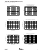
The nine holes in the landing pattern for the OPA567 are for
the thermal vias that connect the thermal pad of the OPA567
to the heatsink area on the PCB. All traces conducting high
currents are very wide for lowest inductance and minimal
resistive losses.