
Datasheet


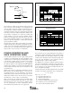


OPA567
SBOS287A
17
www.ti.com
FIGURE 9. Junction-to-Ambient Thermal Resistance with
Various Heatsinking Efforts.
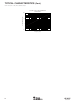
FIGURE 10. Maximum Power Dissipation vs Temperature.
FIGURE 11. Thermal Resistance vs Number of Thermal Vias.
FIGURE 12. Feedback Capacitor for Use with Higher Imped-
ance Networks.
The Maximum Power Dissipation vs Temperature for the
heatsinking methods referenced in Figure 9 is shown in
Figure 10.
FEEDBACK CAPACITOR IMPROVES RESPONSE
For optimum settling time and stability with higher impedance
feedback networks (R
F
> 50kΩ), it may be necessary to add
a feedback capacitor across the feedback resistor, R
F
, as
shown in Figure 12. This capacitor compensates for the zero
created by the feedback network impedance and the input
capacitance of the OPA567 (and any parasitic layout capaci-
tance). The effect becomes more significant with higher
impedance networks.
The size of the capacitor needed is estimated using the
equation:
R
IN
• C
IN
= R
F
• C
F
where C
IN
is the sum of the input capacitance of the OPA567
plus the parasitic layout capacitance.
To appropriately determine required heatsink area, required
power dissipation should be calculated and the relationship
between power dissipation and thermal resistance should be
considered to minimize shutdown conditions and allow for
proper long-term operation (junction temperature of 125°C).
Once the heatsink area has been selected, worst-case load
conditions should be tested to ensure proper thermal protec-
tion.
For applications with limited board size, refer to Figure 11 for
the approximate thermal resistance relative to the number of
thermal vias. The QFN-12 package is well suited for continu-
ous power levels, as shown in Figure 10. Higher power levels
may be achieved in applications with a low on/off duty cycle.
OPA567
V+
V–
V
OUT
V
IN
R
IN
8
1, 12
2, 3
4, 5
9
R
IN
• C
IN
= R
F
•
C
F
R
F
C
L
C
IN
C
IN
C
F
Where C
IN
is equal to the OPA567 input
capacitance (approximately 9pF) plus any
parasitic layout capacitance.
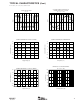
HEATSINKING METHOD
θ
JA
The part is soldered to a 2 oz copper pad under the 38
exposed pad.
Soldered to copper pad with forced airflow (150lfm). 36
Soldered to copper pad with forced airflow (250lfm). 35
Soldered to copper pad with forced airflow (500lfm). 34
6
5
4
3
2
1
0
Temperature (°C)
MAXIMUM POWER DISSIPATION IN PACKAGE
vs TEMPERATURE
Power Dissipated (W)
–75 –50 0–25 25 50 75 100 125
Thermal pad soldered
to 2oz. copper pad,
with 500lfm airlow.
Thermal pad soldered
to 2oz. copper pad,
without forced air.
T
J
= 150°C
100
90
80
70
60
50
40
30
20
10
0
Thermal Resistance, θ
JA
(°C/W)
0123456
Number of Thermal Vias
THERMAL RESISTANCE
vs NUMBER OF THERMAL VIAS