
Datasheet


External
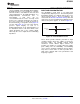
Pin
+V
CC
-V
CC
Internal
Circuitry
OPA3690
www.ti.com
SBOS237G –MARCH 2002–REVISED MARCH 2010
current capability of the OPA3690 allows multiple INPUT AND ESD PROTECTION
destination devices to be handled as separate
The OPA3690 is built using a very high-speed
transmission lines, each with their own series and
complementary bipolar process. The internal junction
shunt terminations. If the 6dB attenuation of a
breakdown voltages are relatively low for these very
doubly-terminated transmission line is
small geometry devices. These breakdowns are
unacceptable, a long trace can be
reflected in the Absolute Maximum Ratings table. All
series-terminated at the source end only. Treat
device pins are protected with internal ESD protection
the trace as a capacitive load in this case and set
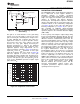
diodes to the power supplies, as shown in Figure 54.
the series resistor value as shown in the plots of
Recommended R
S
vs Capacitive Load (Figure 15
for ±5V and Figure 30 for +5V). This will not
preserve signal integrity as well as a
doubly-terminated line. If the input impedance of
the destination device is low, there will be some
signal attenuation due to the voltage divider
formed by the series output into the terminating
impedance.
Figure 54. Internal ESD Protection
These diodes provide moderate protection to input
overdrive voltages above the supplies as well. The
protection diodes can typically support 30mA
continuous current. Where higher currents are
possible (for example, in systems with ±15V supply
parts driving into the OPA3690), current-limiting
series resistors should be added into the two inputs.
Keep these resistor values as low as possible since
high values degrade both noise performance and
frequency response.
Copyright © 2002–2010, Texas Instruments Incorporated Submit Documentation Feedback 29
Product Folder Link(s): OPA3690