
Datasheet


R
F
402W
±200mVOutputAdjustment
= = 2- -
Power-supply
decouplingnotshown.
5kW
5kW
328W
0.1 Fm
R
G
200W
V
I
1.25kW
10kW
0.1 Fm
-5V
+5V
1/3
OPA3690
+5V
-5V
V
O
V
O
V
I
R
F
R
G
OPA3690
www.ti.com
SBOS237G –MARCH 2002–REVISED MARCH 2010
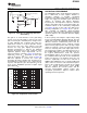
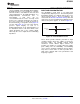
DC ACCURACY AND OFFSET CONTROL a dc current back into the source that must be
considered. Applying an offset adjustment to the
The balanced input stage of a wideband
inverting op amp input can change the noise gain and
voltage-feedback op amp allows good output dc
frequency response flatness. For a dc-coupled
accuracy in a wide variety of applications. The
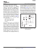
inverting amplifier, Figure 51 shows one example of
power-supply current trim for the OPA3690 gives
an offset adjustment technique that has minimal
even tighter control than comparable amplifiers.
impact on the signal frequency response. In this
Although the high-speed input stage does require
case, the dc offsetting current is brought into the
relatively high input bias current (typically 5mA out of
inverting input node through resistor values that are
each input terminal), the close matching between
much larger than the signal path resistors. This
them may be used to reduce the output dc error
ensures that the adjustment circuit has minimal effect
caused by this current. The total output offset voltage
on the loop gain and hence, the frequency response.
may be considerably reduced by matching the dc
source resistances appearing at the two inputs. This
reduces the output dc error due to the input bias
currents to the offset current times the feedback
resistor. Evaluating the configuration of Figure 36,
and using worst-case +25°C input offset voltage and
current specifications, gives a worst-case output
offset voltage equal to:
– (NG = noninverting signal gain)
±(NG × V
OS(MAX)
) ± (R
F
× I
OS(MAX)
)
= ±(2 × 4.5mV) ± (250Ω × 1mA)
= ±9.25mV
A fine-scale output offset null, or dc operating point
adjustment, is often required. Numerous techniques
are available for introducing dc offset control into an
op amp circuit. Most of these techniques eventually
reduce to adding a dc current through the feedback
resistor. In selecting an offset trim method, one key
consideration is the impact on the desired signal path
frequency response. If the signal path is intended to
be noninverting, the offset control is best applied as
Figure 51. DC-Coupled, Inverting Gain of –2, with
an inverting summing signal to avoid interaction with
Offset Adjustment
the signal source. If the signal path is intended to be
inverting, applying the offset control to the
noninverting input may be considered. However, the
dc offset voltage on the summing junction will set up
Copyright © 2002–2010, Texas Instruments Incorporated Submit Documentation Feedback 25
Product Folder Link(s): OPA3690