
Datasheet


E =
O
E
NI
2
+(I R ) +4kTR
BN S S
2
NG +(I R ) +4kTR NG
2 2
BI F F
E =
N
I R
BI F
NG
E +(I R ) +4kTR +
NI BN S S
22
+
4kTR
F
NG
2
4kT
RG
R
G
R
F
R
S
1/3
OPA3690
I
BI
E
O
I
BN
4kT=1.6E 20J-
at290 K°
E
RS
E
NI
4kTR
S
Ö
4kTRFÖ
OPA3690
SBOS237G –MARCH 2002–REVISED MARCH 2010
www.ti.com
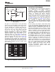
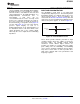
NOISE PERFORMANCE The total output spot noise voltage can be computed
as the square root of the sum of all squared output
High slew rate, unity-gain stable, voltage-feedback op
noise voltage contributors. Equation 4 shows the
amps usually achieve their slew rate at the expense
general form for the output noise voltage using the
of a higher input noise voltage. The 5.5nV/√Hz input
terms shown in Figure 50.
voltage noise for the OPA3690 is, however, much
lower than comparable amplifiers. The input-referred
voltage noise, and the two input-referred current
(4)
noise terms, combine to give low output noise under
a wide variety of operating conditions. Figure 50
Dividing this expression by the noise gain [NG = (1 +
shows the op amp noise analysis model with all the
R
F
/R
G
)] will give the equivalent input-referred spot
noise terms included. In this model, all noise terms
noise voltage at the noninverting input, as shown in
are taken to be noise voltage or current density terms
Equation 5.
in either nV/√Hz or pA/√Hz.
(5)
Evaluating these two equations for the OPA3690
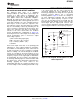
circuit and component values (see Figure 36) gives a
total output spot noise voltage of 12.3nV/√Hz and a
total equivalent input spot noise voltage of 6.1nV/√Hz.
This is including the noise added by the bias current
cancellation resistor (100Ω) on the noninverting input.
This total input-referred spot noise voltage is only
slightly higher than the 5.5nV/√Hz specification for the
op amp voltage noise alone. This will be the case as
long as the impedances appearing at each op amp
input are limited to the previously recommend
maximum value of 300Ω. Keeping both (R
F
|| R
G
) and
the noninverting input source impedance less than
Figure 50. Op Amp Noise Analysis Model
300Ω will satisfy both noise and frequency response
flatness considerations. As the resistor-induced noise
is relatively negligible, additional capacitive
decoupling across the bias current cancellation
resistor (R
B
) for the inverting op amp configuration of
Figure 47 is not required.
24 Submit Documentation Feedback Copyright © 2002–2010, Texas Instruments Incorporated
Product Folder Link(s): OPA3690