
Datasheet


OPA3690
SBOS237G –MARCH 2002–REVISED MARCH 2010
www.ti.com
OUTPUT CURRENT AND VOLTAGE DRIVING CAPACITIVE LOADS
The OPA3690 provides output voltage and current One of the most demanding and yet very common
capabilities that are unsurpassed in a low-cost load conditions for an op amp is capacitive loading.
monolithic op amp. Under no-load conditions at Often, the capacitive load is the input of an
+25°C, the output voltage typically swings closer than ADC—including additional external capacitance which
1V to either supply rail; the specified swing limit is may be recommended to improve ADC linearity. A
within 1.2V of either rail. Into a 15Ω load (the high-speed, high open-loop gain amplifier like the
minimum tested load), it will deliver more than OPA3690 can be very susceptible to decreased
±160mA. stability and closed-loop response peaking when a
capacitive load is placed directly on the output pin.
The specifications described previously, though
When the amplifier's open-loop output resistance is
familiar in the industry, consider voltage and current
considered, this capacitive load introduces an
limits separately. In many applications, it is the
additional pole in the signal path that can decrease
voltage × current, or V-I product, that is more relevant
the phase margin. Several external solutions to this
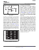
to circuit operation. Refer to Figure 19, the Output
problem have been suggested. When the primary
Voltage and Current Limitations plot in the Typical
considerations are frequency response flatness,
Characteristics. The X- and Y-axes of this graph
pulse response fidelity, and/or distortion, the simplest
show the zero-voltage output current limit and the
and most effective solution is to isolate the capacitive
zero-current output voltage limit, respectively. The
load from the feedback loop by inserting a
four quadrants give a more detailed view of the
series-isolation resistor between the amplifier output
OPA3690 output drive capabilities, noting that the
and the capacitive load. This does not eliminate the
graph is bounded by a Safe Operating Area of 1W
pole from the loop response, but rather shifts it and
maximum internal power dissipation for a single
adds a zero at a higher frequency. The additional
channel. Superimposing resistor load lines onto the
zero acts to cancel the phase lag from the capacitive
plot shows that the OPA3690 can drive ±2.5V into
load pole, thus increasing the phase margin and
25Ω or ±3.5V into 50Ω without exceeding the output
improving stability.
capabilities or the 1W dissipation limit. A 100Ω load
line (the standard test circuit load) shows the full The Typical Characteristics show the recommended
±3.9V output swing capability (see the Electrical R
S
versus capacitive load (Figure 15 for ±5V and
Characteristics). Figure 30 for +5V) and the resulting frequency
response at the load. Parasitic capacitive loads
The minimum specified output voltage and current
greater than 2pF can begin to degrade the
specifications over temperature are set by worst-case
performance of the OPA3690. Long PCB traces,
simulations at the cold temperature extreme. Only at
unmatched cables, and connections to multiple
cold startup will the output current and voltage
devices can easily exceed this value. Always
decrease to the numbers shown in the Electrical
consider this effect carefully, and add the
Characteristic tables. As the output transistors deliver
recommended series resistor as close as possible to
power, their junction temperatures increase,
the OPA3690 output pin (see the Board Layout
decreasing their V
BE
s (increasing the available output
Guidelines section).
voltage swing) and increasing their current gains
(increasing the available output current). In The criterion for setting this R
S
resistor is a maximum
steady-state operation, the available output voltage bandwidth, flat frequency response at the load. For
and current is always greater than that shown in the the OPA3690 operating in a gain of +2, the frequency
over-temperature specifications because the output response at the output pin is already slightly peaked
stage junction temperatures will be higher than the without the capacitive load requiring relatively high
minimum specified operating ambient. values of R
S
to flatten the response at the load.
Increasing the noise gain will reduce the peaking as
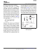
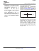
To protect the output stage from accidental shorts to
described previously. The circuit of Figure 48
ground and the power supplies, output short-circuit
demonstrates this technique, allowing lower values of
protection is included in the OPA3690. The circuit
R
S
to be used for a given capacitive load. This was
acts to limit the maximum source or sink current to
used to generate the Recommended R
S
vs
approximately 250mA.
Capacitive Load plots (Figure 15 for ±5V and
Figure 30 for +5V).
22 Submit Documentation Feedback Copyright © 2002–2010, Texas Instruments Incorporated
Product Folder Link(s): OPA3690