
Datasheet


Delay=
2t
1+(2 f )p t
2
,foreachsection.
1/3
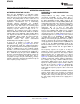
OPA3690
V
1
V
OUT
402W
402W
806W
V
2
200W
402W 402W
200W
1/3
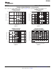
OPA3690
1/3
OPA3690
V =2(V -
OUT 1 2
V )
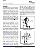
Frequency(MHz)
100 40010
Gain(dB)
10
5
0
-5
-10
-15
-20
Time(200ns/div)
InputandOutputVoltage(200mV/div)
800
600
400
200
0
-200
-400
-600
-800
Output
Input
106ns
OPA3690
SBOS237G –MARCH 2002–REVISED MARCH 2010
www.ti.com
ANALOG DELAY LINE INSTRUMENTATION DIFFERENTIAL
AMPLIFIER
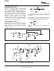
The circuit on the front page of this data sheet shows
an analog delay line using the OPA3690. The first op Figure 41 shows an instrumentation differential
amp buffers the delay line from the source, and can amplifier based on the OPA3690. This application
be used to establish the dc operating point if single benefits from the OPA3690 dc precision,
+5V supply operation is desired. The last two common-mode rejection, high impedance input, and
sections provide an analog delay function given by low-current noise. The resistors on the last
Equation 1: (difference) amplifier were selected to keep the loads
equal on the input stage op amps. The matched
loads and a careful PCB layout can improve
(1)
2nd-harmonic distortion at higher frequencies.
Where: Figure 42 shows the frequency response of the
instrumentation differential amplifier.
t = RC.
f represents the frequency components of interest
in the input signal.
For input frequencies below 0.39/2pt = 2.5MHz, the
delay will be within 15% of the desired value (2t).
The circuit on the front page gives a delay of 50ns
per stage for a total delay of 100ns. Excellent pulse
fidelity will be retained as long as the first five
harmonics are delayed equally. For the circuit on the
front page, the 5th-harmonic should be = 2.5MHz/5,
which will support a square wave up to 500kHz, with
good pulse response. The input rise-and-fall times
also need to be = 0.30/2.5MHz = 120ns in order to
keep the spectral energy within this 2.5MHz limit.
Quicker rise or fall times will cause propagation delay
errors and excessive pre-shoot.
Figure 41. Instrumentation Amplifier
Shorter delays may be implemented at higher
frequencies by adjusting R and C. To maintain bias
current cancellation, it is best to simply reduce C
without changing R. The analog delay line pulse
response is shown in Figure 40.
Figure 42. Frequency Response for the OPA3690
as an Instrumentation Amplifier
In applications where current-feedback amplifiers or
Figure 40. Analog Delay Line Pulse Response
fixed-gain amplifiers can be used, the OPA3691 or
OPA3692 will provide wider bandwidth
The 1pF capacitors limit the noise, while maintaining
instrumentation amplifiers.
good pulse response. If desired, these two capacitors
may be removed for circuits that produce less delay.
16 Submit Documentation Feedback Copyright © 2002–2010, Texas Instruments Incorporated
Product Folder Link(s): OPA3690