
Datasheet
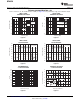
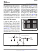


70
68
66
64
62
60
58
56
54
52
50
OutputPull-DownCurrent(mA)
0 1 2 3 4 5 6 7 8 9 10
SFDR(dBc)
V =2V ,10MHz
O PP
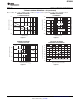
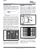
1/3
OPA3690
402W
50W
402W
59W
1V
PP
698W
698W
V
I
+5V
0.1 Fm
R
S
30W
I
B
R
B
50pF
0.1 Fm
2.5VDC
±1VAC
ADCInput
Power-supplydecouplingnotshown.
OPA3690
www.ti.com
SBOS237G –MARCH 2002–REVISED MARCH 2010
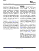
Again, an additional resistor (50Ω in this case) is The OPA3690 in the circuit of Figure 39 provides
included directly in series with the noninverting input. > 200MHz bandwidth for a 2V
PP
output swing.
This minimum recommended value provides part of Minimal 3rd-harmonic distortion or two-tone,
the dc source resistance matching for the 3rd-order intermodulation distortion will be observed
noninverting input bias current. It is also used to form due to the very low crossover distortion in the
a simple parasitic pole to roll off the frequency OPA3690 output stage. The limit of output
response at very high frequencies ( > 500MHz) using Spurious-Free Dynamic Range (SFDR) will be set by
the input parasitic capacitance to form a bandlimiting the 2nd-harmonic distortion. Without R
B
, the circuit of
pole. The gain resistor (R
G
) is ac-coupled, giving the Figure 39 measured at 10MHz shows an SFDR of
circuit a dc gain of +1, which puts the input dc bias 57dBc. This may be improved by pulling additional dc
voltage (2.5V) on the output as well. The output bias current (I
B
) out of the output stage through the
voltage can swing to within 1V of either supply pin optional R
B
resistor to ground (the output midpoint is
while delivering > 100mA output current. A at 2.5V for Figure 39). Adjusting I
B
gives the
demanding 100Ω load to a midpoint bias is used in improvement in SFDR shown in Figure 38. SFDR
this characterization circuit. The new output stage improvement is achieved for I
B
values up to 5mA,
circuit used in the OPA3690 can deliver large bipolar with worse performance for higher values. Using the
output currents into this midpoint load with minimal dual OPA3690 in an I/Q receiver channel will give
crossover distortion, as shown in the ±5V supply matched ac performance through high frequencies.
harmonic distortion plots.
SINGLE-SUPPLY ADC INTERFACE
Most modern, high-performance ADCs (such as the
TI ADS8xx and ADS9xx series from Texas
Instruments) operate on a single +5V (or lower)
power supply. It has been a considerable challenge
for single-supply op amps to deliver a low distortion
input signal at the ADC input for signal frequencies
exceeding 5MHz. The high slew rate, exceptional
output swing, and high linearity of the OPA3690
make it an ideal single-supply ADC driver. The circuit
on the front page shows one possible interface
particularly suited to differential I/O, ac-coupled
requirements. Figure 39 shows the test circuit of
Figure 37 modified for a capacitive (ADC) load and
with an optional output pull-down resistor (R
B
). This
Figure 38. SFDR vs I
B
circuit would be suitable to dual-channel ADC driving
with a single-ended I/O.
Figure 39. Single-Supply ADC Input Driver (one of three channels)
Copyright © 2002–2010, Texas Instruments Incorporated Submit Documentation Feedback 15
Product Folder Link(s): OPA3690