
Datasheet


1/3
OPA3690
+5V
+
DIS
-5V
50W Load
50W
50W
175W
V
O
+V
S
-V
S
V
I
50W Source
R
G
402W
R
F
402W
+
6.8 Fm
0.1 Fm 6.8 Fm
0.1 Fm
0.1 Fm
1/3
OPA3690
+5V
+V
S
DIS
V /2
S
698W
50W
59W
100WV
O
V
I
698W
R
G
402W
R
F
402W
0.1 Fm
0.1 Fm
+
6.8 Fm0.1 Fm
OPA3690
SBOS237G –MARCH 2002–REVISED MARCH 2010
www.ti.com
APPLICATION INFORMATION
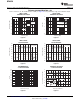
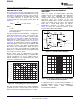
WIDEBAND VOLTAGE-FEEDBACK bandwidth. The key requirement of broadband
OPERATION single-supply operation is to maintain input and
output signal swings within the usable voltage ranges
The OPA3690 provides an exceptional combination
at both the input and the output. The circuit of
of high output power capability in a wideband,
Figure 37 establishes an input midpoint bias using a
unity-gain stable voltage-feedback op amp using a
simple resistive divider from the +5V supply (two
new high slew rate input stage. Typical differential
698Ω resistors). The input signal is then ac-coupled
input stages used for voltage feedback op amps are
into the midpoint voltage bias. The input voltage can
designed to steer a fixed-bias current to the
swing to within 1.5V of either supply pin, giving a
compensation capacitor, setting a limit to the
2V
PP
input signal range centered between the supply
achievable slew rate. The OPA3690 uses a new input
pins. The input impedance matching resistor (59Ω)
stage that places the transconductance element
used for testing is adjusted to give a 50Ω input load
between two input buffers, using their output currents
when the parallel combination of the biasing divider
as the forward signal. As the error voltage increases
network is included.
across the two inputs, an increasing current is
delivered to the compensation capacitor. This
provides very high slew rate (1800V/ms) while
consuming relatively low quiescent current (5.5mA).
This exceptional, full-power performance comes at
the price of a slightly higher input noise voltage than
alternative architectures. The 5.5nV/√Hz input voltage
noise for the OPA3690 is exceptionally low for this
type of input stage.
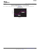
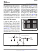
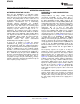
Figure 36 shows the dc-coupled, gain of +2, dual
power supply circuit configuration used as the basis
of the ±5V Electrical Characteristics and Typical
Characteristics. For test purposes, the input
impedance is set to 50Ω with a resistor to ground and
the output impedance is set to 50Ω with a series
output resistor. Voltage swings reported in the
Electrical Characteristics are taken directly at the
input and output pins, while output powers (dBm) are
at the matched 50Ω load. For the circuit of Figure 36,
Figure 36. DC-Coupled, G = +2, Bipolar-Supply
the total effective load will be 100Ω || 804Ω. The
Specification and Test Circuit
disable control line is typically left open for normal
amplifier operation. Two optional components are
included in Figure 36. An additional resistor (100Ω) is
included in series with the noninverting input.
Combined with the 25Ω dc source resistance looking
back towards the signal generator, this gives an input
bias current cancelling resistance that matches the
125Ω source resistance seen at the inverting input
(see the DC Accuracy and Offset Control section). In
addition to the usual power-supply decoupling
capacitors to ground, a 0.1mF capacitor is included
between the two power-supply pins. In practical
printed circuit board (PCB) layouts, this
optional-added capacitor will typically improve the
2nd-harmonic distortion performance by 3dB to 6dB.
Figure 37 shows the ac-coupled, gain of +2,
single-supply circuit configuration used as the basis
of the +5V Electrical Characteristics and Typical
Characteristics. Though not a rail-to-rail design, the
OPA3690 requires minimal input and output voltage
Figure 37. AC-Coupled, G = +2, Single-Supply
headroom compared to other very wideband
Specification and Test Circuit
voltage-feedback op amps. It will deliver a 3V
PP
output swing on a single +5V supply with > 150MHz
14 Submit Documentation Feedback Copyright © 2002–2010, Texas Instruments Incorporated
Product Folder Link(s): OPA3690