
Datasheet


Table Of Contents
www.ti.com
ACHIEVING OUTPUT SWING TO THE OP
GENERAL LAYOUT GUIDELINES
V
OUT
R =20kW
P
OpAmpV =GND-
OPA333
V
IN
V+=+5V
-5V
Additional
Negative
Supply
+ +
+
- -
+
4.096V
0.1 Fm
+5V
ZeroAdj.
K-Type
Thermocouple
40.7 V/ Cm °
R
2
549W
R
9
150kW
R
5
31.6kW
R
1
6.04kW
R
6
200W
+5V
0.1 Fm
R
2
2.94kW
V
O
R
3
60.4W
R
4
6.04kW
OPA333
D1
REF3140
OPA333
OPA2333
SBOS351C – MARCH 2006 – REVISED MAY 2007
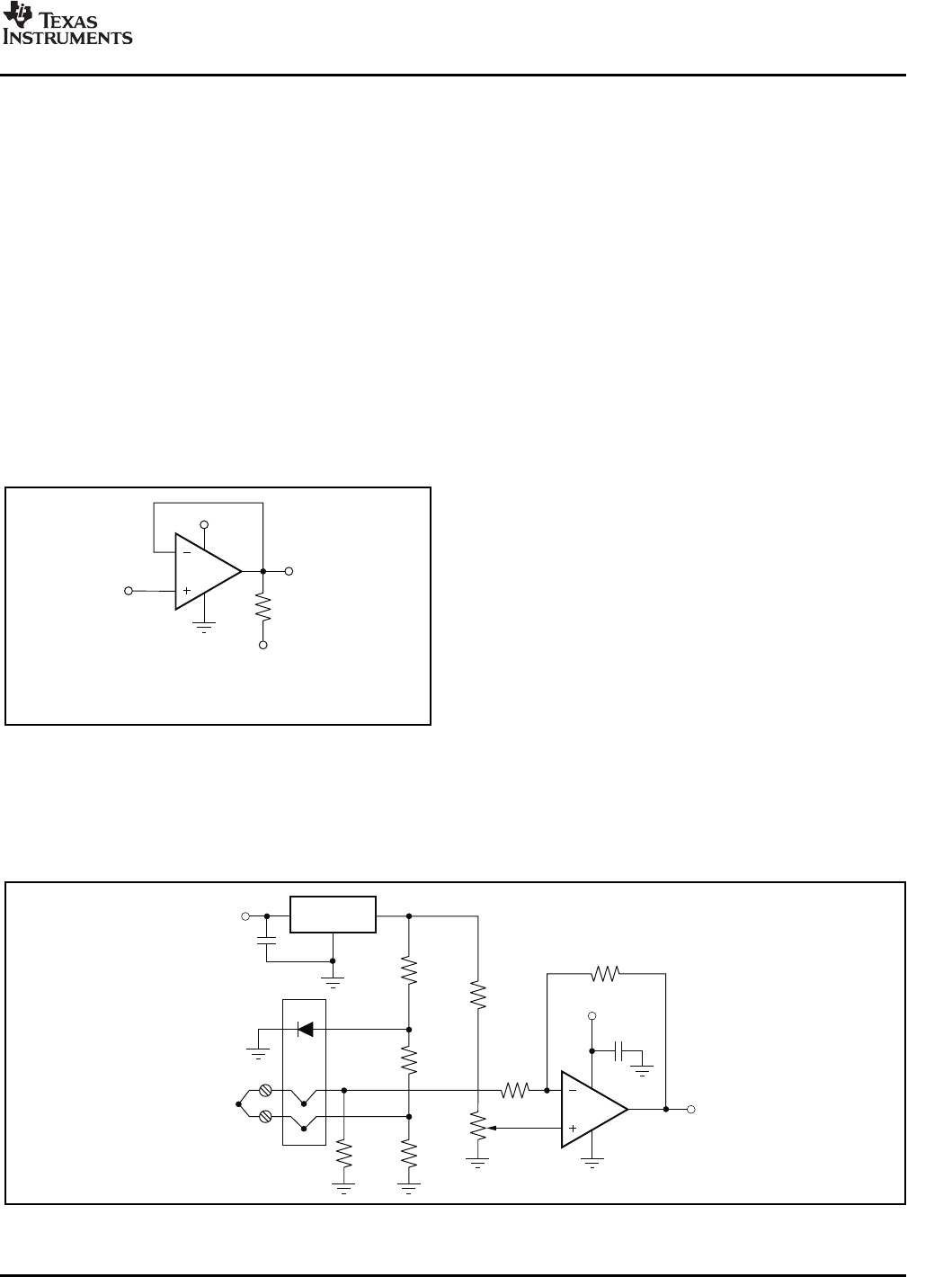
works with some types of output stages. The
AMP NEGATIVE RAIL OPA333 and OPA2333 have been characterized to
perform with this technique; the recommended
Some applications require output voltage swings
resistor value is approximately 20k Ω . Note that this
from 0V to a positive full-scale voltage (such as
configuration will increase the current consumption
+2.5V) with excellent accuracy. With most
by several hundreds of microamps. Accuracy is
single-supply op amps, problems arise when the
excellent down to 0V and as low as –2mV. Limiting
output signal approaches 0V, near the lower output
and nonlinearity occurs below –2mV, but excellent
swing limit of a single-supply op amp. A good
accuracy returns as the output is again driven above
single-supply op amp may swing close to
–2mV. Lowering the resistance of the pull-down
single-supply ground, but will not reach ground. The
resistor will allow the op amp to swing even further
output of the OPA333 and OPA2333 can be made to
below the negative rail. Resistances as low as 10k Ω
swing to ground, or slightly below, on a single-supply
can be used to achieve excellent accuracy down to
power source. To do so requires the use of another
–10mV.
resistor and an additional, more negative, power
supply than the op amp negative supply. A pull-down
resistor may be connected between the output and
the additional negative supply to pull the output down
Attention to good layout practices is always
below the value that the output would otherwise
recommended. Keep traces short and, when
achieve, as shown in Figure 19 .
possible, use a printed circuit board (PCB) ground
plane with surface-mount components placed as
close to the device pins as possible. Place a 0.1 μ F
capacitor closely across the supply pins. These
guidelines should be applied throughout the analog
circuit to improve performance and provide benefits
such as reducing the EMI
(electromagnetic-interference) susceptibility.
Operational amplifiers vary in their susceptibility to
radio frequency interference (RFI). RFI can generally
be identified as a variation in offset voltage or dc
signal levels with changes in the interfering RF
signal. The OPA333 has been specifically designed
to minimize susceptibility to RFI and demonstrates
Figure 19. For V
OUT
Range to Ground
remarkably low sensitivity compared to previous
generation devices. Strong RF fields may still cause
varying offset levels.
The OPA333 and OPA2333 have an output stage
that allows the output voltage to be pulled to its
negative supply rail, or slightly below, using the
technique previously described. This technique only
Figure 20. Temperature Measurement
9
Submit Documentation Feedback