
Datasheet


Table Of Contents
www.ti.com
R
1
V
EX
V
OUT
V
REF
R
1
OPA333
R
R
R R
+5V
NOTE:1%resistorsprovideadequatecommon-moderejectionatsmallground-looperrors.
OPA333
ADS1100
Load
V
I C
2
R
1
4.99kW
R
3
4.99kW
R
4
48.7kW
R
2
49.9kW
+5V
3V
REF3130
R
7
1.18kW
R
SHUNT
1W
R
6
71.5kW
R
N
56W
R
N
56W
(PGAGain=4)
FS=3.0V
StrayGround-LoopResistance
I
LOAD
OPA333
Output
R
SHUNT
Load
V+
V+
R
G
R
L
R
(2)
1
10kW
R
BIAS
+5V
zener
(1)
Twozener
biasingmethods
areshown.
(3)
MOSFETratedto
stand-offsupplyvoltage
suchasBSS84for
upto50V.
(1)zenerratedforopampsupplycapability(thatis,5.1VforOPA333).
(2)Current-limitingresistor.
(3)ChoosezenerbiasingresistorordualNMOSFETs(FDG6301N,NTJD4001N,orSi1034)
NOTES:
OPA333
OPA2333
SBOS351C – MARCH 2006 – REVISED MAY 2007
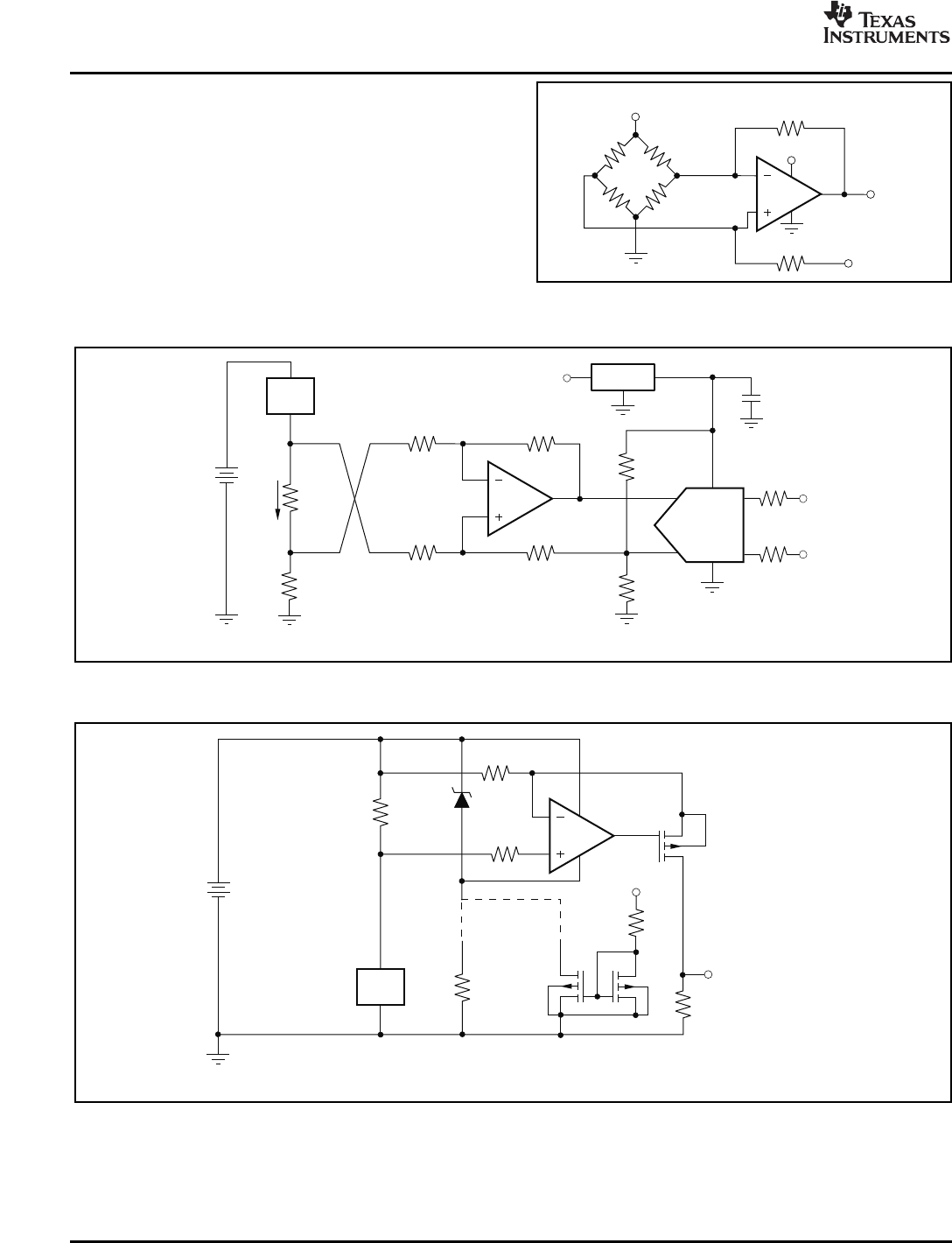
Figure 21 shows the basic configuration for a bridge
amplifier.
A low-side current shunt monitor is shown in
Figure 22 . R
N
are operational resistors used to
isolate the ADS1100 from the noise of the digital I
2
C
bus. Since the ADS1100 is a 16-bit converter, a
precise reference is essential for maximum accuracy.
If absolute accuracy is not required, and the 5V
power supply is sufficiently stable, the REF3130 may
be omitted.
Figure 21. Single Op Amp Bridge Amplifier
Figure 22. Low-Side Current Monitor
Figure 23. High-Side Current Monitor
10
Submit Documentation Feedback