
Datasheet


*+
**
SLOS099E − OCTOBER 1983 − REVISED MAY 2004
4
POST OFFICE BOX 655303 DALLAS, TEXAS 75265
•
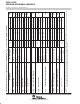
electrical characteristics at specified free-air temperature, V
CC
±
=
±15 V (unless otherwise noted)
PARAMETER
TEST CONDITIONS
†
T
A
OP07C OP07D
UNIT
PARAMETER
TEST CONDITIONS
†
T
A
MIN TYP MAX MIN TYP MAX
UNIT
V
IO
Input offset voltage
V
O
= 0,
R
S
= 50 Ω
25°C 60 150 60 150
V
V
IO
Input offset voltage V
O
= 0, R
S
= 50 Ω
0°C to 70°C
85 250 85 250
µV
a
V
IO
Temperature coefficient of input offset voltage V
O
= 0, R
S
= 50 Ω 0°C to 70°C 0.5 1.8 0.7 2.5 µV/°C
Long-term drift of input offset voltage See Note 6 0.4 0.5 µV/mo
Offset adjustment range R
S
= 20 kΩ, See Figure 1 25°C ±4 ±4 mV
I
IO
Input offset current
25°C 0.8 6 0.8 6
nA
I
IO
Input offset current
0°C to 70°C 1.6 8 1.6 8
nA
a
I
IO
Temperature coefficient of input offset current 0°C to 70°C 12 50 12 50 pA/°C
I
IB
Input bias current
25°C ±1.8 ± 7 ±2 ±12
nA
I
IB
Input bias current
0°C to 70°C ±2.2 ± 9 ±3 ±14
nA
a
I
IB
Temperature coefficient of input bias current 0°C to 70°C 18 50 18 50 pA/°C
V
ICR
Common-mode input voltge range
25°C ±13 ±14 ±13 ±14
V
V
ICR
Common-mode input voltge range
0°C to 70°C ±13 ±13.5 ±13 ±13.5
V
R
L
≥ 10 kΩ ±12 ±13 ±12 ±13
V
OM
Peak output voltage
R
L
≥ 2 kΩ
25°C
±11.5 ±12.8 ±11.5 ±12.8
V
V
OM
Peak output voltage
R
L
≥ 1 kΩ
25 C
±12 ±12
V
R
L
≥ 2 kΩ 0°C to 70°C ±11 ±12.6 ±11 ±12.6
A
VD
Large-signal differential voltage amplification
V
CC±
= ±3 V,
R
L
≥ 500 kΩ
V
O
= ±0.5 V,
25°C 100 400 400
V/mV
A
VD
Large-signal differential voltage amplification
V
O
= ±10 V,
R
L
= 2 kΩ
25°C 120 400 120 400
V/mV
V
O
= ±10 V, R
L
= 2 kΩ
0°C to 70°C
100 400 100 400
B
1
Unity-gain bandwidth 25°C 0.4 0.6 0.4 0.6 MHz
r
i
Input resistance 25°C 8 33 7 31 MΩ
CMRR
Common-mode rejection ratio
V
IC
= ±13 V,
R
S
= 50 Ω
25°C 100 120 94 110
dB
CMRR Common-mode rejection ratio V
IC
= ±13 V
,
R
S
= 50 Ω
0°C to 70°C
97 120 94 106
dB
k
SVS
Supply-voltage sensitivity (∆V
IO
/∆V
CC
)
V
CC±
=
±
3 V to
±
18 V,
25°C 7 32 7 32
V/V
k
SVS
Supply-voltage sensitivity (∆V
IO
/∆V
CC
)
V
CC±
= ±3 V to ±18 V,
R
S
= 50 Ω
0°C to 70°C 10 51 10 51
µV/V
V
O
= 0, No load 80 150 80 150
P
D
Power dissipation
V
CC±
= ±3 V, V
O
= 0,
No load
25°C
4 8 4 8
mW
†
All characteristics are measured under open-loop conditions, with zero common-mode input voltage, unless otherwise noted.
NOTE 7: Since long-term drift cannot be measured on the individual devices prior to shipment, this specification is not intended to be a warranty. It is an engineering estimate of the
averaged trend line of drift versus time over extended periods after the first 30 days of operation.