
User manual


www.ti.com
2.4.14 Clock Enable Control Register (CKEN)
PLL Controller
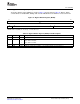
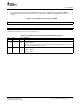
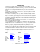
The clock enable control register (CKEN) is shown in Figure 17 and described in Table 23 . CKEN
provides clock enable control for miscellaneous output clocks. CKEN is only applicable to PLLC1, not
PLLC2.
Figure 17. Clock Enable Control Register (CKEN)
31 16
Reserved
R-0
15 2 1 0
Reserved OBSEN AUXEN
R-0 R/W-1 R/W-1
LEGEND: R/W = Read/Write; R = Read only; - n = value after reset
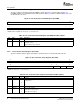
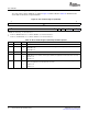
Table 23. Clock Enable Control Register (CKEN) Field Descriptions
Bit Field Value Description
31-2 Reserved 0 Reserved
1 OBSEN OBSCLK enable. Actual OBSCLK status is shown in the clock status register (CKSTAT).
0 OBSCLK is disabled.
1 OBSCLK is enabled. For OBSCLK to toggle, both the OBSEN bit and the OD1EN bit in the oscillator
divider 1 register (OSCDIV1) must be set to 1.
0 AUXEN AUXCLK enable. Actual AUXCLK status is shown in the clock status register (CKSTAT).
0 AUXCLK is disabled.
1 AUXCLK is enabled.
SPRUES0B – December 2007 Phase-Locked Loop Controller (PLLC) 31
Submit Documentation Feedback