
Datasheet

MSP430G2x33
MSP430G2x03
www.ti.com
SLAS734F –APRIL 2011–REVISED MAY 2013
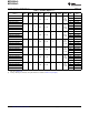
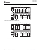
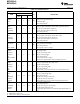
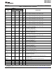
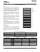
Table 2. Terminal Functions (continued)
TERMINAL
NO.
I/O DESCRIPTION
NAME
PW20,
PW28 RHB32
N20
P2.0/ General-purpose digital I/O pin
8 10 9 I/O
TA1.0 Timer1_A, capture: CCI0A input, compare: Out0 output
P2.1/ General-purpose digital I/O pin
9 11 10 I/O
TA1.1 Timer1_A, capture: CCI1A input, compare: Out1 output
P2.2/ General-purpose digital I/O pin
10 12 11 I/O
TA1.1 Timer1_A, capture: CCI1B input, compare: Out1 output
P2.3/ General-purpose digital I/O pin
11 16 15 I/O
TA1.0 Timer1_A, capture: CCI0B input, compare: Out0 output
P2.4/ General-purpose digital I/O pin
12 17 16 I/O
TA1.2 Timer1_A, capture: CCI2A input, compare: Out2 output
P2.5/ General-purpose digital I/O pin
13 18 17 I/O
TA1.2 Timer1_A, capture: CCI2B input, compare: Out2 output
XIN/ Input terminal of crystal oscillator
P2.6/ 19 27 26 I/O General-purpose digital I/O pin
TA0.1 Timer0_A, compare: Out1 output
XOUT/ Output terminal of crystal oscillator
(3)
18 26 25 I/O
P2.7 General-purpose digital I/O pin
P3.0/ General-purpose digital I/O pin
- 9 7 I/O
TA0.2 Timer0_A, capture: CCI2A input, compare: Out2 output
P3.1/ General-purpose digital I/O pin
- 8 6 I/O
TA1.0 Timer1_A, compare: Out0 output
P3.2/ General-purpose digital I/O pin
- 13 12 I/O
TA1.1 Timer1_A, compare: Out1 output
P3.3/ General-purpose digital I/O
- 14 13 I/O
TA1.2 Timer1_A, compare: Out2 output
P3.4/ General-purpose digital I/O
- 15 14 I/O
TA0.0 Timer0_A, compare: Out0 output
P3.5/ General-purpose digital I/O
- 19 18 I/O
TA0.1 Timer0_A, compare: Out1 output
P3.6/ General-purpose digital I/O
- 20 19 I/O
TA0.2 Timer0_A, compare: Out2 output
P3.7/ General-purpose digital I/O
- 21 20 I/O
TA1CLK Timer1_A, clock signal TACLK input
RST/ Reset
NMI/ 16 24 23 I Nonmaskable interrupt input
SBWTDIO Spy-Bi-Wire test data input/output during programming and test
TEST/ Selects test mode for JTAG pins on Port 1. The device protection fuse is
connected to TEST.
17 25 24 I
SBWTCK Spy-Bi-Wire test clock input during programming and test
AVCC NA NA 29 NA Analog supply voltage
DVCC 1 1 30 NA Digital supply voltage
DVSS 20 28 27, 28 NA Ground reference
NC NA NA 8, 32 NA Not connected
(3) If XOUT/P2.7 is used as an input, excess current flows until P2SEL.7 is cleared. This is due to the oscillator output driver connection to
this pad after reset.
Copyright © 2011–2013, Texas Instruments Incorporated Submit Documentation Feedback 7