
Datasheet

MSP430G2x33
MSP430G2x03
SLAS734F –APRIL 2011–REVISED MAY 2013
www.ti.com
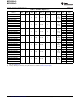
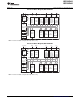
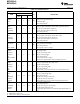
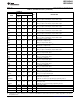
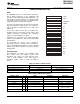
Table 2. Terminal Functions
TERMINAL
NO.
I/O DESCRIPTION
NAME
PW20,
PW28 RHB32
N20
P1.0/ General-purpose digital I/O pin
TA0CLK/ Timer0_A, clock signal TACLK input
2 2 31 I/O
ACLK/ ACLK signal output
A0 ADC10 analog input A0
(1)
P1.1/ General-purpose digital I/O pin
TA0.0/ Timer0_A, capture: CCI0A input, compare: Out0 output / BSL transmit
UCA0RXD/ 3 3 1 I/O USCI_A0 receive data input in UART mode
UCA0SOMI/ USCI_A0 slave data out/master in SPI mode
A1 ADC10 analog input A1
(1)
P1.2/ General-purpose digital I/O pin
TA0.1/ Timer0_A, capture: CCI1A input, compare: Out1 output
UCA0TXD/ 4 4 2 I/O USCI_A0 transmit data output in UART mode
UCA0SIMO/ USCI_A0 slave data in/master out in SPI mode
A2 ADC10 analog input A2
(1)
P1.3/ General-purpose digital I/O pin
ADC10CLK/ ADC10, conversion clock output
(1)
5 5 3 I/O
A3/ ADC10 analog input A3
(1)
VREF-/VEREF- ADC10 negative reference voltage
(1)
P1.4/ General-purpose digital I/O pin
SMCLK/ SMCLK signal output
UCB0STE/ USCI_B0 slave transmit enable
UCA0CLK/ 6 6 4 I/O USCI_A0 clock input/output
A4/ ADC10 analog input A4
(1)
VREF+/VEREF+ ADC10 positive reference voltage
(1)
TCK JTAG test clock, input terminal for device programming and test
P1.5/ General-purpose digital I/O pin
TA0.0/ Timer0_A, compare: Out0 output / BSL receive
UCB0CLK/ USCI_B0 clock input/output
7 7 5 I/O
UCA0STE/ USCI_A0 slave transmit enable
A5/ ADC10 analog input A5
(1)
TMS JTAG test mode select, input terminal for device programming and test
P1.6/ General-purpose digital I/O pin
TA0.1/ Timer0_A, compare: Out1 output
A6/ ADC10 analog input A6
(1)
14 22 21 I/O
UCB0SOMI/ USCI_B0 slave out/master in SPI mode,
UCB0SCL/ USCI_B0 SCL I2C clock in I2C mode
TDI/TCLK JTAG test data input or test clock input during programming and test
P1.7/ General-purpose digital I/O pin
A7/ ADC10 analog input A7
(1)
UCB0SIMO/ USCI_B0 slave in/master out in SPI mode
15 23 22 I/O
UCB0SDA/ USCI_B0 SDA I2C data in I2C mode
TDO/TDI JTAG test data output terminal or test data input during programming and
test
(2)
(1) MSP430G2x33 devices only
(2) TDO or TDI is selected via JTAG instruction.
6 Submit Documentation Feedback Copyright © 2011–2013, Texas Instruments Incorporated