
Datasheet
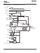
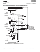
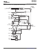

P1.5/TA0.0/UCB0CLK/
UCA0STE/A5*/TMS
P1.6/TA0.1/UCB0SOMI/
UCB0SCL/A6*/TDI/TCLK
P1.7/CAOUT/UCB0SIMO/
UCB0SDA/A7*/TDO/TDI
From Module
From Module
* Note: MSP430G2x33 devices only. MSP430G2x03 devices have no ADC10.
To Module
From Module
PxOUT.y
DV
SS
DV
CC
1
TAx.y
TAxCLK
Bus
Keeper
EN
1
0
PxIN.y
EN
D
PxSEL.y
PxREN.y
1
0
PxSEL2.y
1
0
INCHx = y *
To ADC10 *
PxSEL.y
1
3
2
1
0
PxSEL2.y
From JTAG
To JTAG
PxIRQ.y
PxIE.y
EN
Set
Q
Interrupt
Edge
Select
PxSEL.y
PxIES.y
PxIFG.y
Direction
0: Input
1: Output
PxDIR.y
From Module
PxSEL.y
3
2
1
0
PxSEL2.y
ADC10AE0.y *
MSP430G2x33
MSP430G2x03
www.ti.com
SLAS734F –APRIL 2011–REVISED MAY 2013
Port P1 Pin Schematic: P1.5 to P1.7, Input/Output With Schmitt Trigger
Copyright © 2011–2013, Texas Instruments Incorporated Submit Documentation Feedback 45