
Datasheet

MSP430G2x33
MSP430G2x03
SLAS734F –APRIL 2011–REVISED MAY 2013
www.ti.com
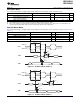
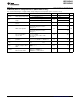
10-Bit ADC, External Reference
(1)
(MSP430G2x33 Only)
over recommended ranges of supply voltage and operating free-air temperature (unless otherwise noted)
PARAMETER TEST CONDITIONS V
CC
MIN TYP MAX UNIT
VEREF+ > VEREF–,
1.4 V
CC
SREF1 = 1, SREF0 = 0
Positive external reference input
VEREF+ V
voltage range
(2)
VEREF– ≤ VEREF+ ≤ V
CC
– 0.15 V,
1.4 3
SREF1 = 1, SREF0 = 1
(3)
Negative external reference input
VEREF– VEREF+ > VEREF– 0 1.2 V
voltage range
(4)
Differential external reference
ΔVEREF input voltage range, VEREF+ > VEREF–
(5)
1.4 V
CC
V
ΔVEREF = VEREF+ – VEREF–
0 V ≤ VEREF+ ≤ V
CC
,
3 V ±1
SREF1 = 1, SREF0 = 0
I
VEREF+
Static input current into VEREF+ µA
0 V ≤ VEREF+ ≤ V
CC
– 0.15 V ≤ 3 V,
3 V 0
SREF1 = 1, SREF0 = 1
(3)
I
VEREF–
Static input current into VEREF– 0 V ≤ VEREF– ≤ V
CC
3 V ±1 µA
(1) The external reference is used during conversion to charge and discharge the capacitance array. The input capacitance, C
I
, is also the
dynamic load for an external reference during conversion. The dynamic impedance of the reference supply should follow the
recommendations on analog-source impedance to allow the charge to settle for 10-bit accuracy.
(2) The accuracy limits the minimum positive external reference voltage. Lower reference voltage levels may be applied with reduced
accuracy requirements.
(3) Under this condition the external reference is internally buffered. The reference buffer is active and requires the reference buffer supply
current I
REFB
. The current consumption can be limited to the sample and conversion period with REBURST = 1.
(4) The accuracy limits the maximum negative external reference voltage. Higher reference voltage levels may be applied with reduced
accuracy requirements.
(5) The accuracy limits the minimum external differential reference voltage. Lower differential reference voltage levels may be applied with
reduced accuracy requirements.
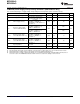
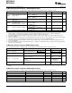
10-Bit ADC, Timing Parameters (MSP430G2x33 Only)
over recommended ranges of supply voltage and operating free-air temperature (unless otherwise noted)
PARAMETER TEST CONDITIONS V
CC
MIN TYP MAX UNIT
ADC10SR = 0 0.45 6.3
ADC10 input clock For specified performance of
f
ADC10CLK
3 V MHz
frequency ADC10 linearity parameters
ADC10SR = 1 0.45 1.5
ADC10 built-in oscillator ADC10DIVx = 0, ADC10SSELx = 0,
f
ADC10OSC
3 V 3.7 6.3 MHz
frequency f
ADC10CLK
= f
ADC10OSC
ADC10 built-in oscillator, ADC10SSELx = 0,
3 V 2.06 3.51
f
ADC10CLK
= f
ADC10OSC
t
CONVERT
Conversion time µs
13 ×
f
ADC10CLK
from ACLK, MCLK, or SMCLK:
ADC10DIV ×
ADC10SSELx ≠ 0
1/f
ADC10CLK
Turn-on settling time of
t
ADC10ON
(1)
100 ns
the ADC
(1) The condition is that the error in a conversion started after t
ADC10ON
is less than ±0.5 LSB. The reference and input signal are already
settled.
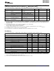
10-Bit ADC, Linearity Parameters (MSP430G2x33 Only)
over recommended ranges of supply voltage and operating free-air temperature (unless otherwise noted)
PARAMETER TEST CONDITIONS V
CC
MIN TYP MAX UNIT
E
I
Integral linearity error 3 V ±1 LSB
E
D
Differential linearity error 3 V ±1 LSB
E
O
Offset error Source impedance R
S
< 100 Ω 3 V ±1 LSB
E
G
Gain error 3 V ±1.1 ±2 LSB
E
T
Total unadjusted error 3 V ±2 ±5 LSB
36 Submit Documentation Feedback Copyright © 2011–2013, Texas Instruments Incorporated