
Datasheet

t
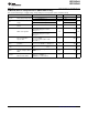
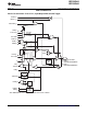
SU,MI
t
HD,MI
UCLK
SOMI
SIMO
t
VALID,MO
CKPL = 0
CKPL = 1
1/f
UCxCLK
t
HD,MO
t
LO/HI
t
LO/HI
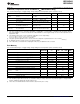
t
SU,MI
t
HD,MI
UCLK
SOMI
SIMO
t
VALID,MO
t
HD,MO
CKPL = 0
CKPL = 1
t
LO/HI
t
LO/HI
1/f
UCxCLK
MSP430G2x33
MSP430G2x03
www.ti.com
SLAS734F –APRIL 2011–REVISED MAY 2013
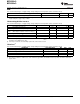
USCI (UART Mode)
over recommended ranges of supply voltage and operating free-air temperature (unless otherwise noted)
PARAMETER TEST CONDITIONS V
CC
MIN TYP MAX UNIT
f
USCI
USCI input clock frequency SMCLK, duty cycle = 50% ± 10% f
SYSTEM
MHz
Maximum BITCLK clock frequency
f
max,BITCLK
3 V 2 MHz
(equals baudrate in MBaud)
(1)
t
τ
UART receive deglitch time
(2)
3 V 50 100 600 ns
(1) The DCO wake-up time must be considered in LPM3 and LPM4 for baud rates above 1 MHz.
(2) Pulses on the UART receive input (UCxRX) shorter than the UART receive deglitch time are suppressed. To ensure that pulses are
correctly recognized, their width should exceed the maximum specification of the deglitch time.
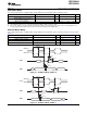
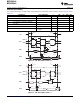
USCI (SPI Master Mode)
over recommended ranges of supply voltage and operating free-air temperature (unless otherwise noted) (see Figure 16 and
Figure 17)
PARAMETER TEST CONDITIONS V
CC
MIN TYP MAX UNIT
f
USCI
USCI input clock frequency SMCLK, duty cycle = 50% ± 10% f
SYSTEM
MHz
t
SU,MI
SOMI input data setup time 3 V 75 ns
t
HD,MI
SOMI input data hold time 3 V 0 ns
t
VALID,MO
SIMO output data valid time UCLK edge to SIMO valid, C
L
= 20 pF 3 V 20 ns
Figure 16. SPI Master Mode, CKPH = 0
Figure 17. SPI Master Mode, CKPH = 1
Copyright © 2011–2013, Texas Instruments Incorporated Submit Documentation Feedback 31