
Datasheet


MSP430G2x33
MSP430G2x03
www.ti.com
SLAS734F –APRIL 2011–REVISED MAY 2013
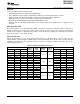
Peripheral File Map
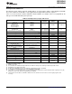
Table 14. Peripherals With Word Access
REGISTER
MODULE REGISTER DESCRIPTION OFFSET
NAME
ADC10 ADC data transfer start address ADC10SA 1BCh
(MSP430G2x33 devices only)
ADC memory ADC10MEM 1B4h
ADC control register 1 ADC10CTL1 1B2h
ADC control register 0 ADC10CTL0 1B0h
Timer1_A3 Capture/compare register TA1CCR2 0196h
Capture/compare register TA1CCR1 0194h
Capture/compare register TA1CCR0 0192h
Timer_A register TA1R 0190h
Capture/compare control TA1CCTL2 0186h
Capture/compare control TA1CCTL1 0184h
Capture/compare control TA1CCTL0 0182h
Timer_A control TA1CTL 0180h
Timer_A interrupt vector TA1IV 011Eh
Timer0_A3 Capture/compare register TA0CCR2 0176h
Capture/compare register TA0CCR1 0174h
Capture/compare register TA0CCR0 0172h
Timer_A register TA0R 0170h
Capture/compare control TA0CCTL2 0166h
Capture/compare control TA0CCTL1 0164h
Capture/compare control TA0CCTL0 0162h
Timer_A control TA0CTL 0160h
Timer_A interrupt vector TA0IV 012Eh
Flash Memory Flash control 3 FCTL3 012Ch
Flash control 2 FCTL2 012Ah
Flash control 1 FCTL1 0128h
Watchdog Timer+ Watchdog/timer control WDTCTL 0120h
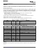
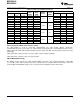
Table 15. Peripherals With Byte Access
REGISTER
MODULE REGISTER DESCRIPTION OFFSET
NAME
USCI_B0 USCI_B0 transmit buffer UCB0TXBUF 06Fh
USCI_B0 receive buffer UCB0RXBUF 06Eh
USCI_B0 status UCB0STAT 06Dh
USCI B0 I2C Interrupt enable UCB0CIE 06Ch
USCI_B0 bit rate control 1 UCB0BR1 06Bh
USCI_B0 bit rate control 0 UCB0BR0 06Ah
USCI_B0 control 1 UCB0CTL1 069h
USCI_B0 control 0 UCB0CTL0 068h
USCI_B0 I2C slave address UCB0SA 011Ah
USCI_B0 I2C own address UCB0OA 0118h
Copyright © 2011–2013, Texas Instruments Incorporated Submit Documentation Feedback 17