
Datasheet


MSP430G2x33
MSP430G2x03
SLAS734F –APRIL 2011–REVISED MAY 2013
www.ti.com
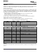
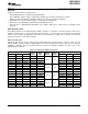
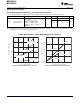
Table 13. Timer1_A3 Signal Connections
INPUT PIN NUMBER DEVICE MODULE MODULE OUTPUT PIN NUMBER
MODULE
INPUT INPUT OUTPUT
BLOCK
PW20, N20 PW28 RHB32 PW20, N20 PW28 RHB32
SIGNAL NAME SIGNAL
- P3.7-21 P3.7-20 TACLK TACLK
ACLK ACLK
Timer NA
SMCLK SMCLK
- P3.7-21 P3.7-20 TACLK INCLK
P2.0-8 P2.0-10 P2.0-9 TA1.0 CCI0A P2.0-8 P2.0-10 P2.0-9
P2.3-11 P2.3-16 P2.3-12 TA1.0 CCI0B P2.3-11 P2.3-16 P2.3-15
CCR0 TA0
V
SS
GND P3.1-8 P3.1-6
V
CC
V
CC
P2.1-9 P2.1-11 P2.1-10 TA1.1 CCI1A P2.1-9 P2.1-11 P2.1-10
P2.2-10 P2.2-12 P2.2-11 TA1.1 CCI1B P2.2-10 P2.2-12 P2.2-11
CCR1 TA1
V
SS
GND P3.2-13 P3.2-12
V
CC
V
CC
P2.4-12 P2.4-17 P2.4-16 TA1.2 CCI2A P2.4-12 P2.4-17 P2.4-16
P2.5-13 P2.5-18 P2.5-17 TA1.2 CCI2B P2.5-13 P2.5-18 P2.5-17
CCR2 TA2
V
SS
GND P3.3-14 P3.3-13
V
CC
V
CC
Universal Serial Communications Interface (USCI)
The USCI module is used for serial data communication. The USCI module supports synchronous
communication protocols such as SPI (3 or 4 pin) and I2C, and asynchronous communication protocols such as
UART, enhanced UART with automatic baudrate detection (LIN), and IrDA. Not all packages support the USCI
functionality.
USCI_A0 provides support for SPI (3 or 4 pin), UART, enhanced UART, and IrDA.
USCI_B0 provides support for SPI (3 or 4 pin) and I2C.
ADC10 (MSP430G2x33 Only)
The ADC10 module supports fast 10-bit analog-to-digital conversions. The module implements a 10-bit SAR
core, sample select control, reference generator, and data transfer controller (DTC) for automatic conversion
result handling, allowing ADC samples to be converted and stored without any CPU intervention.
16 Submit Documentation Feedback Copyright © 2011–2013, Texas Instruments Incorporated