
Datasheet


MSP430G2x33
MSP430G2x03
www.ti.com
SLAS734F –APRIL 2011–REVISED MAY 2013
Digital I/O
Up to three 8-bit I/O ports are implemented:
• All individual I/O bits are independently programmable.
• Any combination of input, output, and interrupt condition (port P1 and port P2 only) is possible.
• Edge-selectable interrupt input capability for all bits of port P1 and port P2 (if available).
• Read/write access to port-control registers is supported by all instructions.
• Each I/O has an individually programmable pullup/pulldown resistor.
• Each I/O has an individually programmable pin oscillator enable bit to enable low-cost capacitive touch
detection.
WDT+ Watchdog Timer
The primary function of the watchdog timer (WDT+) module is to perform a controlled system restart after a
software problem occurs. If the selected time interval expires, a system reset is generated. If the watchdog
function is not needed in an application, the module can be disabled or configured as an interval timer and can
generate interrupts at selected time intervals.
Timer_A3 (TA0, TA1)
Timer0_A3 and Timer1_A3 are 16-bit timers/counters with three capture/compare registers. Timer_A3 can
support multiple capture/compares, PWM outputs, and interval timing. Timer_A3 also has extensive interrupt
capabilities. Interrupts may be generated from the counter on overflow conditions and from each of the
capture/compare registers.
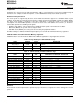
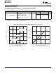
Table 12. Timer0_A3 Signal Connections
INPUT PIN NUMBER DEVICE MODULE MODULE OUTPUT PIN NUMBER
MODULE
INPUT INPUT OUTPUT
BLOCK
PW20, N20 PW28 RHB32 PW20, N20 PW28 RHB32
SIGNAL NAME SIGNAL
P1.0-2 P1.0-2 P1.0-31 TACLK TACLK
ACLK ACLK
Timer NA
SMCLK SMCLK
PinOsc PinOsc PinOsc TACLK INCLK
P1.1-3 P1.1-3 P1.1-1 TA0.0 CCI0A P1.1-3 P1.1-3 P1.1-1
ACLK CCI0B P1.5-7 P1.5-7 P1.5-5
CCR0 TA0
V
SS
GND - P3.4-15 P3.4-14
V
CC
V
CC
P1.2-4 P1.2-4 P1.2-2 TA0.1 CCI1A P1.2-4 P1.2-4 P1.2-2
CAOUT CCI1B P1.6-14 P1.6-22 P1.6-21
CCR1 TA1
V
SS
GND P2.6-19 P2.6-27 P2.6-26
V
CC
V
CC
- P3.5-19 P3.5-18
- P3.0-9 P3.0-7 TA0.2 CCI2A - P3.0-9 P3.0-7
PinOsc PinOsc PinOsc TA0.2 CCI2B - P3.6-20 P3.6-19
CCR2 TA2
V
SS
GND
V
CC
V
CC
Copyright © 2011–2013, Texas Instruments Incorporated Submit Documentation Feedback 15