
Datasheet


MSP430G2x33
MSP430G2x03
SLAS734F –APRIL 2011–REVISED MAY 2013
www.ti.com
Peripherals
Peripherals are connected to the CPU through data, address, and control buses and can be handled using all
instructions. For complete module descriptions, see the MSP430x2xx Family User's Guide (SLAU144).
Oscillator and System Clock
The clock system is supported by the basic clock module that includes support for a 32768-Hz watch crystal
oscillator, an internal very-low-power low-frequency oscillator and an internal digitally controlled oscillator (DCO).
The basic clock module is designed to meet the requirements of both low system cost and low power
consumption. The internal DCO provides a fast turn-on clock source and stabilizes in less than 1 µs. The basic
clock module provides the following clock signals:
• Auxiliary clock (ACLK), sourced either from a 32768-Hz watch crystal or the internal LF oscillator.
• Main clock (MCLK), the system clock used by the CPU.
• Sub-Main clock (SMCLK), the sub-system clock used by the peripheral modules.
The DCO settings to calibrate the DCO output frequency are stored in the information memory segment A.
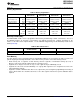
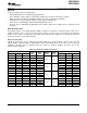
Calibration Data Stored in Information Memory Segment A
Calibration data is stored for both the DCO and for ADC10 organized in a tag-length-value structure.
Table 10. Tags Used by the ADC Calibration Tags
NAME ADDRESS VALUE DESCRIPTION
DCO frequency calibration at V
CC
= 3 V and T
A
= 30°C at
TAG_DCO_30 0x10F6 0x01
calibration
TAG_ADC10_1 0x10DA 0x10 ADC10_1 calibration tag
TAG_EMPTY - 0xFE Identifier for empty memory areas
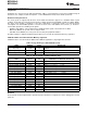
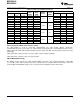
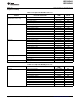
Table 11. Labels Used by the ADC Calibration Tags
ADDRESS
LABEL SIZE CONDITION AT CALIBRATION / DESCRIPTION
OFFSET
CAL_ADC_25T85 0x0010 word INCHx = 0x1010, REF2_5 = 1, T
A
= 85°C
CAL_ADC_25T30 0x000E word INCHx = 0x1010, REF2_5 = 1, T
A
= 30°C
CAL_ADC_25VREF_FACTOR 0x000C word REF2_5 = 1, T
A
= 30°C, I
VREF+
= 1 mA
CAL_ADC_15T85 0x000A word INCHx = 0x1010, REF2_5 = 0, T
A
= 85°C
CAL_ADC_15T30 0x0008 word INCHx = 0x1010, REF2_5 = 0, T
A
= 30°C
CAL_ADC_15VREF_FACTOR 0x0006 word REF2_5 = 0, T
A
= 30°C, I
VREF+
= 0.5 mA
CAL_ADC_OFFSET 0x0004 word External VREF = 1.5 V, f
ADC10CLK
= 5 MHz
CAL_ADC_GAIN_FACTOR 0x0002 word External VREF = 1.5 V, f
ADC10CLK
= 5 MHz
CAL_BC1_1MHZ 0x0009 byte -
CAL_DCO_1MHZ 0x0008 byte -
CAL_BC1_8MHZ 0x0007 byte -
CAL_DCO_8MHZ 0x0006 byte -
CAL_BC1_12MHZ 0x0005 byte -
CAL_DCO_12MHZ 0x0004 byte -
CAL_BC1_16MHZ 0x0003 byte -
CAL_DCO_16MHZ 0x0002 byte -
Brownout
The brownout circuit is implemented to provide the proper internal reset signal to the device during power on and
power off.
14 Submit Documentation Feedback Copyright © 2011–2013, Texas Instruments Incorporated