
Datasheet


OA0
+
−
OA1
+
−
(V2 − V1) × R2
R1
Vdiff =
R2R1
V2
V1
OA Operation
www.ti.com
NOTE: Using OAx Negative Input Simultaneously as ADC Input
When the pin connected to the negative input multiplexer is also used as an input to the
ADC, conversion errors up to 5 mV may be observed due to internal wiring voltage drops.
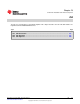
20.2.4.8 Differential Amplifier Mode
This mode allows internal routing of the OA signals for a two-opamp or three-opamp instrumentation
amplifier. Figure 20-2 shows a two-opamp configuration with OA0 and OA1. In this mode the output of the
OAx is connected to R
TOP
by routing through another OAx in the Inverting PGA mode. R
BOTTOM
is
unconnected providing a unity gain buffer. This buffer is combined with one or two remaining OAx to form
the differential amplifier. The OAx output is connected to the ADC input channel as selected by the
OAxCTL0 bits.
Figure 20-2 shows an example of a two-opamp differential amplifier using OA0 and OA1. The control
register settings and are shown in Table 20-3. The gain for the amplifier is selected by the OAFBRx bits
for OA1 and is shown in Table 20-4. The OAx interconnections are shown in Figure 20-3.
Table 20-3. Two-Opamp Differential Amplifier Control
Register Settings
Settings
Register
(binary)
OA0CTL0 xx xx xx 0 0
OA0CTL1 000 111 0 x
OA1CTL0 11 xx xx x x
OA1CTL1 xxx 110 0 x
Table 20-4. Two-Opamp Differential Amplifier Gain
Settings
OA1 OAFBRx Gain
000 0
001 1/3
010 1
011 1 2/3
100 3
101 4 1/3
110 7
111 15
Figure 20-2. Two-Opamp Differential Amplifier
516
OA SLAU144J–December 2004–Revised July 2013
Submit Documentation Feedback
Copyright © 2004–2013, Texas Instruments Incorporated