
Datasheet

MF10-N
www.ti.com
SNOS547C –JUNE 1999–REVISED APRIL 2013
Operating Ratings
(1)
Temperature Range (T
MIN
≤ T
A
≤ T
MAX
) MF10ACN, MF10CCN, MF10CCWM 0°C ≤ T
A
≤ 70°C
(1) Absolute Maximum Ratings indicate limits beyond which damage to the device may occur. DC and AC electrical specifications do not
apply when operating the device beyond its specified operating conditions.
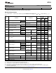
Electrical Characteristics
V
+
= +5.00V and V
−
= −5.00V unless otherwise specified. Boldface limits apply for T
MIN
to T
MAX
; all other limits T
A
= T
J
=
25°C.
MF10ACN, MF10CCN,
MF10CCWM
Symbol Parameter Conditions Units
Tested Design
Typical
(1)
Limit
(2)
Limit
(3)
V
+
− V
−
Min 9 V
Supply Voltage
Max 14
I
S
Clock Applied to Pins 10 & 11
Maximum Supply Current 8 12 12 mA
No Input Signal
f
O
Min f
O
× Q < 200 kHz 0.1 0.2 Hz
Center Frequency Range
Max 30 20 kHz
f
CLK
Min 5.0 10 Hz
Clock Frequency Range
Max 1.5 1.0 MHz
f
CLK
/f
O
MF10A V
pin12
= 5V ±0.2 ±0.6 ±0.6
50:1 Clock to Center Frequency
Q = 10, Mode 1 f
CLK
= 250
Ratio Deviation
MF10C ±0.2 ±1.5 ±1.5
KHz
%
f
CLK
/f
O
MF10A V
pin12
= 0V ±0.2 ±0.6 ±0.6
100:1 Clock to Center Frequency
Q = 10, Mode 1
f
CLK
= 500 kHz
Ratio Deviation
MF10C ±0.2 ±1.5 ±1.5
Clock Feedthrough Q = 10, Mode 1 10 mV
V
pin12
= 5V
±2 ±6 ±6
f
CLK
= 250 kHz
Q Error (MAX)
(4)
Q = 10, Mode 1 %
V
pin12
= 0V
±2 ±6 ±6
f
CLK
= 500 kHz
H
OLP
DC Lowpass Gain Mode 1 R1 = R2 = 10k 0 ±0.2 ±0.2 dB
V
OS1
DC Offset Voltage
(5)
±5.0 ±20 ±20 mV
V
OS2
Min V
pin12
= +5V S
A/B
= V
+
−150 −185 −185
mV
(f
CLK
/f
O
= 50)
Max −85 −85
DC Offset Voltage
(5)
Min V
pin12
= +5V S
A/B
= V
−
−70 mV
(f
CLK
/f
O
= 50)
Max
V
OS3
Min V
pin12
= +5V All Modes −70 −100 −100
DC Offset Voltage
(5)
mV
(f
CLK
/f
O
= 50)
Max −20 −20
V
OS2
V
pin12
= 0V S
A/B
= V
+
−300 mV
(f
CLK
/f
O
= 100)
DC Offset Voltage
(5)
V
pin12
= 0V S
A/B
= V
−
−140 mV
(f
CLK
/f
O
= 100)
V
OS3
V
pin12
= 0V All Modes
DC Offset Voltage
(5)
−140 mV
(f
CLK
/f
O
= 100)
V
OUT
Minimum Output BP, LP Pins R
L
= 5k ±4.25 ±3.8 ±3.8 V
Voltage Swing N/AP/HP Pin R
L
= 3.5k ±4.25 ±3.8 ±3.8 V
GBW Op Amp Gain BW Product 2.5 MHz
SR Op Amp Slew Rate 7 V/μs
(1) Typicals are at 25°C and represent most likely parametric norm.
(2) Tested limits are ensured to AOQL (Average Outgoing Quality Level).
(3) Design limits are specified but not 100% tested. These limits are not used to calculate outgoing quality levels.
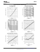
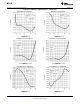
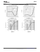
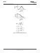
(4) The accuracy of the Q value is a function of the center frequency (f
O
). This is illustrated in the curves under the heading “Typical
Performance Characteristics”.
(5) V
OS1
, V
OS2
, and V
OS3
refer to the internal offsets as discussed in OFFSET VOLTAGE.
Copyright © 1999–2013, Texas Instruments Incorporated Submit Documentation Feedback 3
Product Folder Links: MF10-N