
Datasheet


MF10-N
SNOS547C –JUNE 1999–REVISED APRIL 2013
www.ti.com
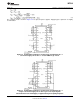
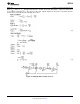
Figure 36. Method for Trimming V
OS
For most applications, the outputs are AC coupled and DC offsets are not bothersome unless large signals are
applied to the filter input. However, larger offset voltages will cause clipping to occur at lower AC signal levels,
and clipping at any of the outputs will cause gain nonlinearities and will change f
O
and Q. When operating in
Mode 3, offsets can become excessively large if R2 and R4 are used to make f
CLK
/f
O
significantly higher than the
nominal value, especially if Q is also high. An extreme example is a bandpass filter having unity gain, a Q of 20,
and f
CLK
/f
O
= 250 with pin 12 tied to ground (100:1 nominal). R4/R2 will therefore be equal to 6.25 and the offset
voltage at the lowpass output will be about +1V. Where necessary, the offset voltage can be adjusted by using
the circuit of Figure 36. This allows adjustment of V
OS1
, which will have varying effects on the different outputs as
described in the above equations. Some outputs cannot be adjusted this way in some modes, however (V
OS(BP)
in modes 1a and 3, for example).
SAMPLED DATA SYSTEM CONSIDERATIONS
The MF10-N is a sampled data filter, and as such, differs in many ways from conventional continuous-time filters.
An important characteristic of sampled-data systems is their effect on signals at frequencies greater than one-
half the sampling frequency. (The MF10-N's sampling frequency is the same as its clock frequency.) If a signal
with a frequency greater than one-half the sampling frequency is applied to the input of a sampled data system, it
will be “reflected” to a frequency less than one-half the sampling frequency. Thus, an input signal whose
frequency is f
s
/2 + 100 Hz will cause the system to respond as though the input frequency was f
s
/2 − 100 Hz.
This phenomenon is known as “aliasing”, and can be reduced or eliminated by limiting the input signal spectrum
to less than f
s
/2. This may in some cases require the use of a bandwidth-limiting filter ahead of the MF10-N to
limit the input spectrum. However, since the clock frequency is much higher than the center frequency, this will
often not be necessary.
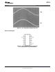
Another characteristic of sampled-data circuits is that the output signal changes amplitude once every sampling
period, resulting in “steps” in the output voltage which occur at the clock rate (Figure 37). If necessary, these can
be “smoothed” with a simple R–C low-pass filter at the MF10-N output.
The ratio of f
CLK
to f
C
(normally either 50:1 or 100:1) will also affect performance. A ratio of 100:1 will reduce any
aliasing problems and is usually recommended for wideband input signals. In noise sensitive applications,
however, a ratio of 50:1 may be better as it will result in 3 dB lower output noise. The 50:1 ratio also results in
lower DC offset voltages, as discussed in OFFSET VOLTAGE.
The accuracy of the f
CLK
/f
O
ratio is dependent on the value of Q. This is illustrated in Typical Performance
Characteristics. As Q is changed, the true value of the ratio changes as well. Unless the Q is low, the error in
f
CLK
/f
O
will be small. If the error is too large for a specific application, use a mode that allows adjustment of the
ratio with external resistors.
It should also be noted that the product of Q and f
O
should be limited to 300 kHz when f
O
< 5 kHz, and to 200
kHz for f
O
> 5 kHz.
26 Submit Documentation Feedback Copyright © 1999–2013, Texas Instruments Incorporated
Product Folder Links: MF10-N