
Datasheet


MF10-N
www.ti.com
SNOS547C –JUNE 1999–REVISED APRIL 2013
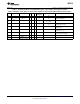
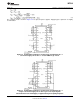
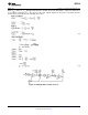
When S
A/B
is tied to V
−
, V
os2
will approximately halve. The DC offset at the BP output is equal to the input offset
of the lowpass integrator (V
os3
). The offsets at the other outputs depend on the mode of operation and the
resistor ratios, as described in the following expressions.
(18)
(19)
Figure 35. MF10-N Offset Voltage Sources
Copyright © 1999–2013, Texas Instruments Incorporated Submit Documentation Feedback 25
Product Folder Links: MF10-N