
Datasheet


MF10-N
SNOS547C –JUNE 1999–REVISED APRIL 2013
www.ti.com
APPLICATIONS INFORMATION
The MF10-N is a general-purpose dual second-order state variable filter whose center frequency is proportional
to the frequency of the square wave applied to the clock input (f
CLK
). By connecting pin 12 to the appropriate DC
voltage, the filter center frequency f
O
can be made equal to either f
CLK
/100 or f
CLK
/50. f
O
can be very accurately
set (within ±6%) by using a crystal clock oscillator, or can be easily varied over a wide frequency range by
adjusting the clock frequency. If desired, the f
CLK
/f
O
ratio can be altered by external resistors as in Figure 25,
Figure 26, Figure 27, Figure 29, Figure 30, and Figure 31. The filter Q and gain are determined by external
resistors.
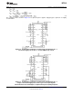
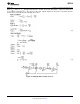
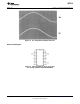
All of the five second-order filter types can be built using either section of the MF10-N. These are illustrated in
Figure 17 through Figure 21 along with their transfer functions and some related equations. Figure 22 shows the
effect of Q on the shapes of these curves. When filter orders greater than two are desired, two or more MF10-N
sections can be cascaded.
DESIGN EXAMPLE
In order to design a second-order filter section using the MF10-N, we must define the necessary values of three
parameters: f
0
, the filter section's center frequency; H
0
, the passband gain; and the filter's Q. These are
determined by the characteristics required of the filter being designed.
As an example, let's assume that a system requires a fourth-order Chebyshev low-pass filter with 1 dB ripple,
unity gain at DC, and 1000 Hz cutoff frequency. As the system order is four, it is realizable using both second-
order sections of an MF10-N. Many filter design texts include tables that list the characteristics (f
O
and Q) of each
of the second-order filter sections needed to synthesize a given higher-order filter. For the Chebyshev filter
defined above, such a table yields the following characteristics:
f
0A
= 529 HzQ
A
= 0.785
f
0B
= 993 HzQ
B
= 3.559
For unity gain at DC, we also specify:
H
0A
= 1
H
0B
= 1
The desired clock-to-cutoff-frequency ratio for the overall filter of this example is 100 and a 100 kHz clock signal
is available. Note that the required center frequencies for the two second-order sections will not be obtainable
with clock-to-center-frequency ratios of 50 or 100. It will be necessary to adjust
(15)
externally. From Table 1, we see that Mode 3 can be used to produce a low-pass filter with resistor-adjustable
center frequency.
In most filter designs involving multiple second-order stages, it is best to place the stages with lower Q values
ahead of stages with higher Q, especially when the higher Q is greater than 0.707. This is due to the higher
relative gain at the center frequency of a higher-Q stage. Placing a stage with lower Q ahead of a higher-Q stage
will provide some attenuation at the center frequency and thus help avoid clipping of signals near this frequency.
For this example, stage A has the lower Q (0.785) so it will be placed ahead of the other stage.
For the first section, we begin the design by choosing a convenient value for the input resistance: R
1A
= 20k. The
absolute value of the passband gain H
OLPA
is made equal to 1 by choosing R
4A
such that: R
4A
= −H
OLPA
R
1A
= R
1A
= 20k. If the 50/100/CL pin is connected to mid-supply for nominal 100:1 clock-to-center-frequency ratio, we find
R
2A
by:
(16)
The resistors for the second section are found in a similar fashion:
22 Submit Documentation Feedback Copyright © 1999–2013, Texas Instruments Incorporated
Product Folder Links: MF10-N