
Datasheet


LP2950-N, LP2951-N
www.ti.com
SNVS764N –JANUARY 2000–REVISED MAY 2013
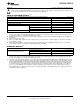
ELECTRICAL CHARACTERISTICS
(1)
(continued)
LP2950AC-XX LP2950C-XX
LP2951
LP2951AC-XX LP2951C-XX
Parameter Conditions
(1)
Units
Typ Tested Typ Tested Design Typ Tested Design
Limit
(2)(3)
Limit
(2)
Limit
(4)
Limit
(2)
Limit
(4)
Load Regulation
(7)
100 μA ≤ I
L
≤ 100 mA 0.04 0.1 0.04 0.1 0.1 0.2 % max
0.3 0.2 0.3 % max
Dropout Voltage
(9)
I
L
= 100 μA 80 80 80 mV
max
50 150 50 150 50 150 mV
max
I
L
= 100 mA 450 450 450 mV
max
380 600 380 600 380 600 mV
max
Ground Current I
L
= 100 μA 75 120 75 120 75 120 μA max
140 140 140 μA max
I
L
= 100 mA 8 12 8 12 8 12 mA
max
14 14 14 mA
max
Dropout Ground V
in
= (V
O
NOM − 0.5)V 110 170 110 170 110 170 μA max
Current I
L
= 100 μA
200 200 200 μA max
Current Limit V
out
= 0 160 200 160 200 160 200 mA
max
220 220 220 mA
max
Thermal Regulation See
(10)
0.05 0.2 0.05 0.2 0.05 0.2 %/W
max
Output Noise, 10 Hz to C
L
= 1μF (5V Only) 430 430 430 μV rms
100 kHz
C
L
= 200 μF 160 160 160 μV rms
C
L
= 3.3 μF 100 100 100 μV rms
(Bypass = 0.01 μF
Pins 7 to 1 (LP2951-N)
8-pin Versions Only LP2951 LP2951AC-XX LP2951C-XX
Reference Voltage 1.23 1.25 1.23 1.25 1.23 1.26 V max
5 5 5
1.26 1.26 1.27 V max
1.22 1.22 1.21 V min
1.2 1.2 1.2 V min
Reference Voltage See
(11)
1.27 1.27 1.285 V max
1.19 1.19 1.185 V min
Feedback Pin Bias 20 40 20 40 20 40 nA max
Current
60 60 60 nA max
Reference Voltage See
(12)
20 20 50 ppm/°C
Temperature
Coefficient
Feedback Pin Bias 0.1 0.1 0.1 nA/°C
Current Temperature
Coefficient
(9) Dropout Voltage is defined as the input to output differential at which the output voltage drops 100 mV below its nominal value
measured at 1V differential. At very low values of programmed output voltage, the minimum input supply voltage of 2V (2.3V over
temperature) must be taken into account.
(10) Thermal regulation is defined as the change in output voltage at a time T after a change in power dissipation is applied, excluding load
or line regulation effects. Specifications are for a 50 mA load pulse at V
IN
= 30V (1.25W pulse) for T = 10ms.
(11) V
REF
≤ V
OUT
≤ (V
IN
− 1V), 2.3V ≤ V
IN
≤ 30V, 100 μA ≤ I
L
≤ 100 mA, T
J
≤ T
JMAX
.
(12) Output or reference voltage temperature coefficient is defined as the worst case voltage change divided by the total temperature range.
Copyright © 2000–2013, Texas Instruments Incorporated Submit Documentation Feedback 5
Product Folder Links: LP2950-N LP2951-N