
Datasheet


R11
1 MW
R8
4.3 kW
R6
10 kW
R5
10 kW
R7
10 kW
VBIAS
(from the
Level Shifter)
I
PHOTO
A2
A1
A3
A4
A5
V+
V-
VREF
VOUT
VREF
VLOGOUT
High-Current Linearity
Correction Signal
I
REF
+
VCC
5 V
C1
100 nF
I
I
2
1
V =
LOGOUT
0.375 LOG
10
·
+ 2 V + I R
1 S
·
(
(
LOG114EVM
www.ti.com
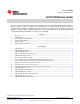
The V
LOGOUT
output is then scaled by resistors R7 and R8. These resistors divide the signal before
combining with the high-current linearity correction section. Combining the input signal and linearity
correction signal is accomplished with amplifier A4 and resistors R5 and R6. Capacitor C1 is used to
bypass the power supply for the LOG114. The signal path circuit is shown in Figure 3.
Figure 3. LOG114EVM Signal Path
2.3 High-Current Linearity Correction
The LOG114 is capable of handling a wide dynamic range of currents, from less than 100 pA in a carefully
designed PCB to 10 mA in high-current applications. Because the LOG114 was designed for high speeds,
the transistors that provide feedback around amplifiers A1 and A2 within the LOG114 have a small series
resistance, R
S
. This small series resistance causes a deviation from the ideal LOG114 transfer function at
input currents that exceed approximately 1 mA. The modified equation for V
LOGOUT
that shows this
deviation from the ideal is given in Equation 3.
(3)
4
LOG114EVM User Guide SBOU110– September 2011
Submit Documentation Feedback
Copyright © 2011, Texas Instruments Incorporated