
Datasheet


Table Of Contents
- FEATURES
- APPLICATIONS
- DESCRIPTION
- Electrical Specifications
- Performance Benefits
- Absolute Maximum Ratings
- Operating Ratings
- Electrical Characteristics
- Typical Performance Characteristics
- Block Diagram
- Design Steps for the LMZ22005 Application
- ENABLE DIVIDER, RENT, RENB AND RENHSELECTION
- OUTPUT VOLTAGE SELECTION
- SOFT-START CAPACITOR SELECTION
- TRACKING SUPPLY DIVIDER OPTION
- CO SELECTION
- CIN SELECTION
- POWER DISSIPATION AND BOARD THERMAL REQUIREMENTS
- PC BOARD LAYOUT GUIDELINES
- Additional Features
- Typical Application Schematic Diagram
- Power Module SMT Guidelines
- Revision History
LMZ22005
www.ti.com
SNVS686I –MARCH 2011–REVISED OCTOBER 2013
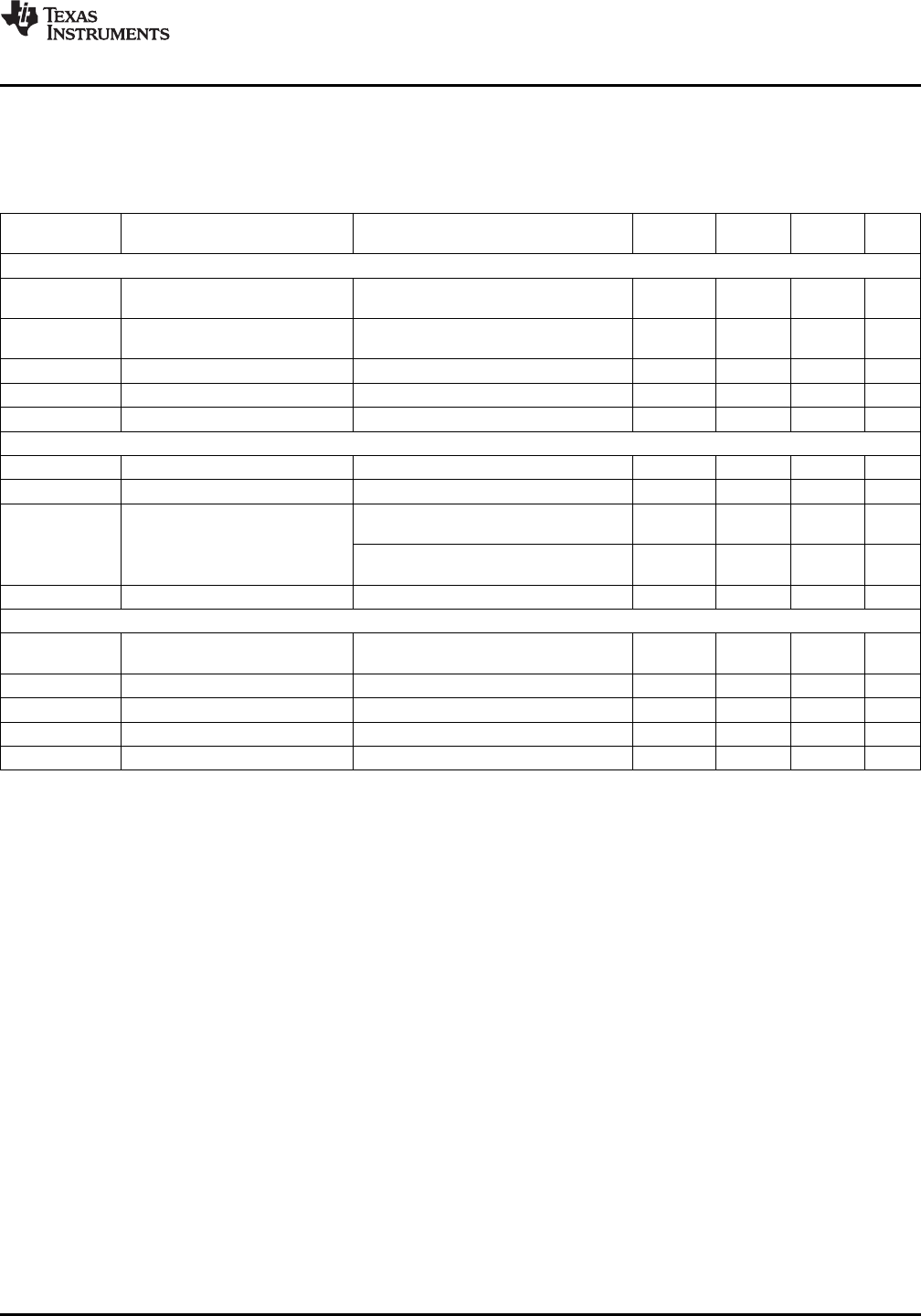
Electrical Characteristics (continued)
Limits in standard type are for T
J
= 25°C only; limits in boldface type apply over the junction temperature (T
J
) range of -40°C
to +125°C. Minimum and Maximum limits are guaranteed through test, design or statistical correlation. Typical values
represent the most likely parametric norm at T
J
= 25°C, and are provided for reference purposes only. Unless otherwise
stated the following conditions apply: V
IN
= 12V, Vout = 3.3V
Min Typ Max
Symbol Parameter Conditions Units
(1) (2) (1)
Regulation and Over-Voltage Comparator
V
FB
In-regulation feedback voltage V
SS
>+ 0.8V 0.776 0.796 0.816 V
I
O
= 5A
V
FB-OV
Feedback over-voltage protection 0.86 V
threshold
I
FB
Feedback input bias current 5 nA
I
Q
Non Switching Input Current V
FB
= 0.86V 2.6 mA
I
SD
Shut Down Quiescent Current V
EN
= 0V 70 μA
Thermal Characteristics
T
SD
Thermal Shutdown Rising 165 °C
T
SD-HYST
Thermal shutdown hysteresis Falling 15 °C
θ
JA
Junction to Ambient
(3)
4 layer Evaluation Printed Circuit Board, 19.3 °C/W
60 vias, No air flow
2 layer JEDEC Printed Circuit Board, No 21.5 °C/W
air flow
θ
JC
Junction to Case No air flow 1.9 °C/W
PERFORMANCE PARAMETERS
(4)
ΔV
O
Output voltage ripple Cout = 220uF w/ 7 milliohm ESR + 9 mV
PP
100uF X5R + 2 x 0.047uF BW@ 20 MHz
ΔV
O
/ΔV
IN
Line regulation V
IN
= 12V to 20V, I
O
= 0.001A ±0.02 %
ΔV
O
/ΔI
OUT
Load regulation V
IN
= 12V, Io=0.001A to 5A 1 mV/A
η Peak efficiency V
IN
= 12V V
O
= 3.3V I
O
= 1A 86 %
η Full load efficiency V
IN
= 12V V
O
= 3.3V I
O
= 5A 81.5 %
(3) Theta JA measured on a 3.5” x 3.5 ” four layer board, with three ounce copper on outer layers and two ounce copper on inner layers,
sixty thermal vias, no air flow, and 1W power dissipation. Refer to application note layout diagrams.
(4) Refer to BOM in Typical Application Bill of Materials.
Copyright © 2011–2013, Texas Instruments Incorporated Submit Documentation Feedback 5
Product Folder Links: LMZ22005