
Datasheet


Table Of Contents
- FEATURES
- APPLICATIONS
- DESCRIPTION
- Electrical Specifications
- Performance Benefits
- Absolute Maximum Ratings
- Operating Ratings
- Electrical Characteristics
- Typical Performance Characteristics
- Block Diagram
- Design Steps for the LMZ22005 Application
- ENABLE DIVIDER, RENT, RENB AND RENHSELECTION
- OUTPUT VOLTAGE SELECTION
- SOFT-START CAPACITOR SELECTION
- TRACKING SUPPLY DIVIDER OPTION
- CO SELECTION
- CIN SELECTION
- POWER DISSIPATION AND BOARD THERMAL REQUIREMENTS
- PC BOARD LAYOUT GUIDELINES
- Additional Features
- Typical Application Schematic Diagram
- Power Module SMT Guidelines
- Revision History
100 mV/Div 500 µs/Div
2A/Div
10 mV/Div 500 ns/Div
0 1 2 3 4 5
0.998
0.999
1.000
1.001
1.002
NORMALLIZED OUTPUT VOLTAGE (V/V)
OUTPUT CURRENT (A)
9 Vin
12 Vin
20 Vin
10 mV/Div 500 ns/Div
30 40 50 60 70 80 90 100 110 120 130
0
1
2
3
4
5
6
MAXIMUM OUTPUT CURRENT (A)
AMBIENT TEMPERATURE (°C)
JA=12°C/W
30 40 50 60 70 80 90 100 110 120 130
0
1
2
3
4
5
6
MAXIMUM OUTPUT CURRENT (A)
AMBIENT TEMPERATURE (°C)
JA = 12 °C/W
LMZ22005
SNVS686I –MARCH 2011–REVISED OCTOBER 2013
www.ti.com
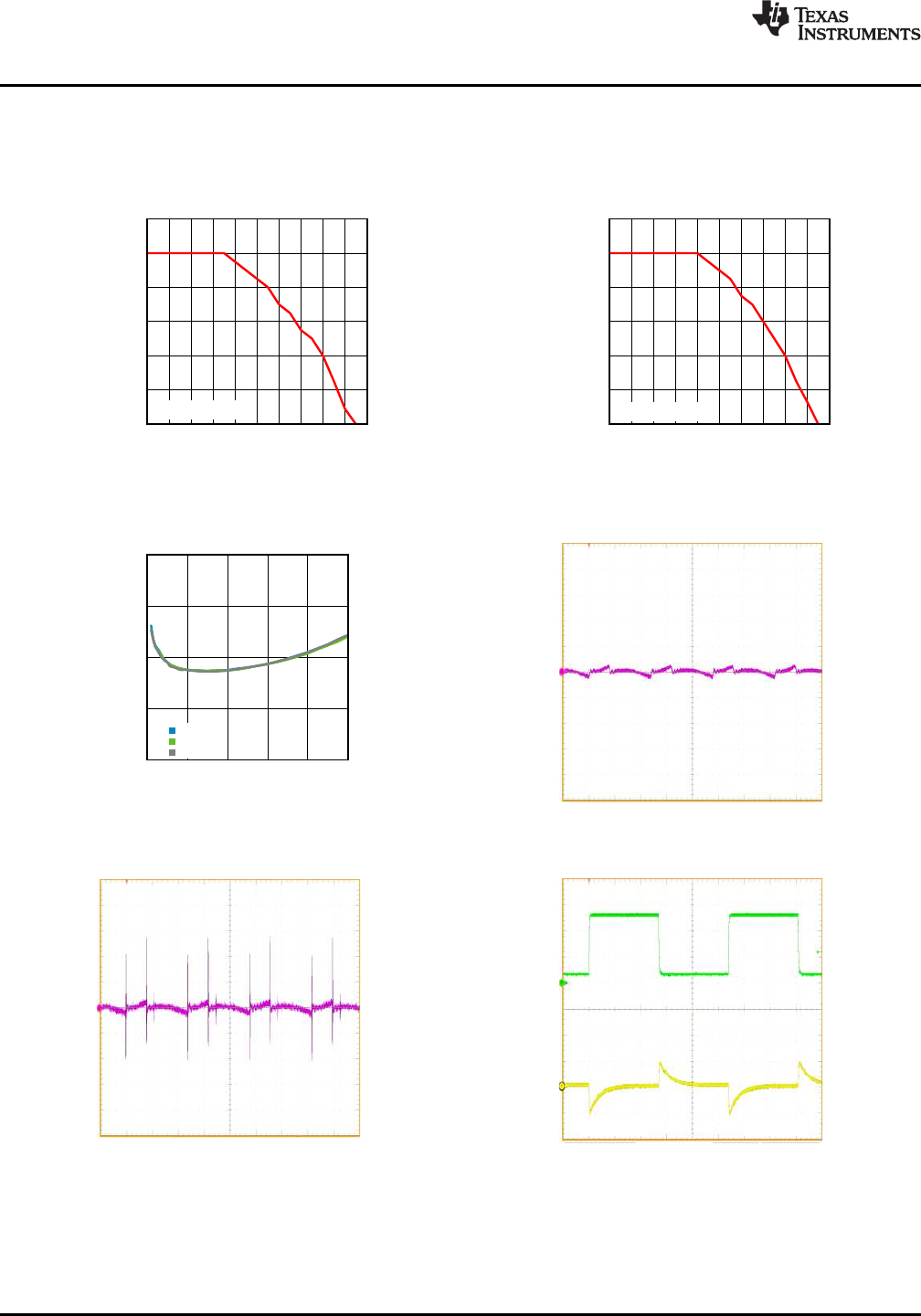
Typical Performance Characteristics (continued)
Unless otherwise specified, the following conditions apply: V
IN
= 12V; Cin = 2 x 10μF + 1μF X7R Ceramic; C
O
= 220μF
Specialty Polymer + 10 uF Ceramic; Tambient = 25° C for waveforms. Efficiency and dissipation plots marked with * have
cycle skipping at light loads resulting is slightly higher output ripple – See Design Steps for the LMZ22005 Application section.
Thermal Derating V
IN
= 12V, V
OUT
= 5.0V Thermal Derating V
IN
= 12V, V
OUT
= 3.3V
Figure 39. Figure 40.
Output Ripple
Normalized — Line and Load Regulation V
OUT
= 3.3V 12V
IN
3.3V
O
@ 5A, BW = 20 MHz
Figure 41. Figure 42.
Output Ripple Transient Response From Evaluation Board
12V
IN
3.3V
O
@ 5A BW = 250 MHz 12V
IN
3.3V
O
0.5 to 5A Step
Figure 43. Figure 44.
12 Submit Documentation Feedback Copyright © 2011–2013, Texas Instruments Incorporated
Product Folder Links: LMZ22005