
Datasheet


Table Of Contents
- FEATURES
- APPLICATIONS
- DESCRIPTION
- Electrical Specifications
- Performance Benefits
- Absolute Maximum Ratings
- Operating Ratings
- Electrical Characteristics
- Typical Performance Characteristics
- Block Diagram
- Design Steps for the LMZ22005 Application
- ENABLE DIVIDER, RENT, RENB AND RENHSELECTION
- OUTPUT VOLTAGE SELECTION
- SOFT-START CAPACITOR SELECTION
- TRACKING SUPPLY DIVIDER OPTION
- CO SELECTION
- CIN SELECTION
- POWER DISSIPATION AND BOARD THERMAL REQUIREMENTS
- PC BOARD LAYOUT GUIDELINES
- Additional Features
- Typical Application Schematic Diagram
- Power Module SMT Guidelines
- Revision History
LMZ22005
www.ti.com
SNVS686I –MARCH 2011–REVISED OCTOBER 2013
LMZ22005 5A SIMPLE SWITCHER® Power Module with 20V Maximum Input Voltage
Check for Samples: LMZ22005
1
FEATURES
DESCRIPTION
2
• Integrated Shielded Inductor
The LMZ22005 SIMPLE SWITCHER© power module
• Simple PCB Layout
is an easy-to-use step-down DC-DC solution capable
of driving up to 5A load. The LMZ22005 is available
• Frequency Synchronization Input (650 kHz to
in an innovative package that enhances thermal
950 kHz)
performance and allows for hand or machine
• Flexible Startup Sequencing Using External
soldering.
Soft-start, Tracking and Precision Enable
The LMZ22005 can accept an input voltage rail
• Protection Against Inrush Currents and Faults
between 6V and 20V and deliver an adjustable and
such as Input UVLO and Output Short Circuit
highly accurate output voltage as low as 0.8V. The
• – 40°C to 125°C Junction Temperature Range
LMZ22005 only requires two external resistors and
three external capacitors to complete the power
• Single Exposed Pad for Easy Mounting and
solution. The LMZ22005 is a reliable and robust
Manufacturing
design with the following protection features: thermal
• Fast Transient Response for Powering FPGAs
shutdown, input under-voltage lockout, output over-
and ASICs
voltage protection, short-circuit protection, output
• Fully Enabled for Webench® Power Designer
current limit, and allows startup into a pre-biased
output. The sync input allows synchronization over
• Pin Compatible with
the 650 to 950 kHz switching frequency range.
LMZ23605/LMZ23603/LMZ22003
ELECTRICAL SPECIFICATIONS
APPLICATIONS
• 30W Maximum Total Output Power
• Point of Load Conversions from 12V Input Rail
• Up to 5A Output Current
• Time Critical Projects
• Input Voltage Range 6V to 20V
• Space Constrained / High Thermal
Requirement Applications • Output Voltage Range 0.8V to 6V
• Negative Output Voltage Applications • Efficiency up to 92%
(see AN-2027 SNVA425)
PERFORMANCE BENEFITS
• High Efficiency Reduces System Heat
Generation
• Complies with EN55022 Class B
(1)
• Low Component Count, Only 5 External
Components
• Low Output Voltage Ripple
• Uses PCB as Heat Sink, no Airflow Required
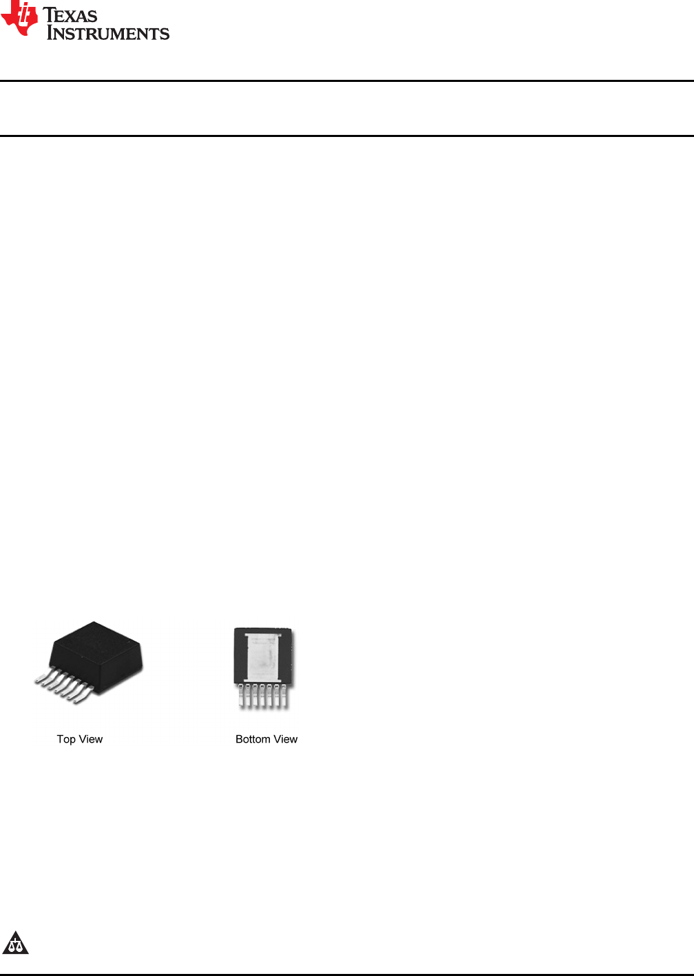
Figure 1. Easy to use 7 pin package
10.16 x 13.77 x 4.57 mm (0.4 x 0.542 x 0.18 in)
θJA = 12°C/W, θJC = 1.9°C/W
RoHS Compliant
(1) EN 55022:2006, +A1:2007, FCC Part 15 Subpart B: 2007.
Peak Reflow Case Temp = 245°C
See AN-2125 SNVA473 and layout for information on device
Power Module SMT Guidelines under test. Vin = 12V, Vo = 3.3V, Io = 5A
1
Please be aware that an important notice concerning availability, standard warranty, and use in critical applications of
Texas Instruments semiconductor products and disclaimers thereto appears at the end of this data sheet.
2All trademarks are the property of their respective owners.
PRODUCTION DATA information is current as of publication date.
Copyright © 2011–2013, Texas Instruments Incorporated
Products conform to specifications per the terms of the Texas
Instruments standard warranty. Production processing does not
necessarily include testing of all parameters.