
Datasheet

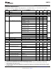


Table Of Contents
LMH6514
SNOSB06A –JANUARY 2008–REVISED MARCH 2013
www.ti.com
5V Electrical Characteristics
(1)
(continued)
The following specifications apply for single supply with V
CC
= 5V, Maximum Gain , R
L
= 100Ω (200Ω external || 200Ω
internal), V
OUT
= 2 V
PP
, fin = 150 MHz. Boldface limits apply at temperature extremes.
Symbol Parameter Conditions Min Typ Max Units
(2) (3) (2)
Maximum Differential Output V
CC
= 5V, Output Common Mode = 5V 5.5 V
PP
Voltage Swing
V
OS
Output Offset Voltage All Gain Settings −21 mV
CMRR Common Mode Rejection Ratio Maximum Gain 81 dB
PSRR Power Supply Rejection Ratio Maximum Gain 63 81
dB
61
Gain Parameters
Maximum Gain DC, Internal R
L
= 186Ω, 29.3 30 30.3
dB
External R
L
= 1280Ω 28.7 30.9
Minimum Gain DC, Internal R
L
= 186Ω, −12.75 −12 −11.85
dB
External R
L
= 1280Ω −13.15 −11.45
Gain Step Size DC 6.02 dB
Gain Step Error DC 0.02
dB
f = 150 MHz 0.07
Cumulative Gain Step Error DC, Gain Step 7 to Gain Step 0 −0.35 0.02 0.30
dB
−0.50 0.45
Gain Step Switching Time 5 ns
Digital Inputs/Timing
Logic Compatibility CMOS Logic 3.3 V
VIL Logic Input Low Voltage 0.8 V
VIH Logic Input High Voltage 2.0 V
IIH Logic Input High Input Current
(4)
Digital Input Voltage = 3.3V 33 40 μA
TSU Setup Time 3 ns
THOLD Hold Time 3 ns
TPW Minimum Latch Pulse Width 10 ns
Power Requirements
ICC Total Supply Current V
OUT
= 0V Differential, V
OUT
Common 107 124
mA
Mode = 5V 134
Amplifier Supply Current Pin 3 Only 56 66
mA
74
Output Stage Bias Currents Pins 13, 14 and Pins 15, 16; 51 58
mA
V
OUT
Common Mode = 5 V 60
(4) Negative input current implies current flowing out of the device.
4 Submit Documentation Feedback Copyright © 2008–2013, Texas Instruments Incorporated
Product Folder Links: LMH6514