
Datasheet
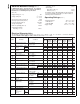


Logic Input Characteristics
Boldface limits apply for T
MIN
to T
MAX
; all other limits T
A
=T
J
= 25˚C.
Parameter Conditions
LMF100CCN LMF100CIWM
Units
Typical Tested Design Typical Tested Design
(Note 8) Limit Limit (Note 8) Limit Limit
(Note 9) (Note 10) (Note 9) (Note 10)
CMOS Clock MIN Logical “1” V
+
= +5V, V
−
= −5V, +3.0 +3.0 +3.0 V
Input Voltage MAX Logical “0” V
LSh
= 0V −3.0 −3.0 −3.0 V
MIN Logical “1” V
+
= +10V, V
−
= 0V, +8.0 +8.0 +8.0 V
MAX Logical “0” V
LSh
= +5V +2.0 +2.0 +2.0 V
TTL Clock MIN Logical “1” V
+
= +5V, V
−
= −5V, +2.0 +2.0 +2.0 V
Input Voltage MAX Logical “0” V
LSh
= 0V +0.8 +0.8 +0.8 V
MIN Logical “1” V
+
= +10V, V
−
= 0V, +2.0 +2.0 +2.0 V
MAX Logical “0” V
LSh
= 0V +0.8 +0.8 +0.8 V
CMOS Clock MIN Logical “1” V
+
= +2.5V, V
−
= −2.5V, +1.5 +1.5 +1.5 V
Input Voltage MAX Logical “0” V
LSh
= 0V −1.5 −1.5 −1.5 V
MIN Logical “1” V
+
= +5V, V
−
= 0V, +4.0 +4.0 +4.0 V
MAX Logical “0” V
LSh
= +2.5V +1.0 +1.0 +1.0 V
TTL Clock MIN Logical “1” V
+
= +5V, V
−
= 0V, +2.0 +2.0 +2.0 V
Input Voltage MAX Logical “0” V
LSh
= 0V, V
D
+
= 0V +0.8 +0.8 +0.8 V
Note 1: Absolute Maximum Ratings indicate limits beyond which damage to the device may occur. Operating Ratings indicate conditions for which the device is in-
tended to be functional. These ratings do not guarantee specific performance limits, however. For guaranteed specifications and test conditions, see the Electrical
Characteristics. The guaranteed specifications apply only for the test conditions listed. Some performance characteristics may degrade when the device is not op-
erated under the listed test conditions.
Note 2: When the input voltage (V
IN
) at any pin exceeds the power supply rails (V
IN
<
V
−
or V
IN
>
V
+
) the absolute value of current at that pin should be limited
to 5 mA or less. The sum of the currents at all pins that are driven beyond the power supply voltages should not exceed 20 mA.
Note 3: The maximum power dissipation must be derated at elevated temperatures and is dictated by T
JMAX
, θ
JA
, and the ambient temperature, T
A
. The maximum
allowable power dissipation at any temperature is P
D
=(T
JMAX
−T
A
)/θ
JA
or the number given in the Absolute Maximum Ratings, whichever is lower. For this device,
T
JMAX
= 125˚C, and the typical junction-to-ambient thermal resistance of the LMF100CIN when board mounted is 55˚C/W. For the LMF100CIWM this number is
66˚C/W.
Note 4: The accuracy of the Q value is a function of the center frequency (f
0
). This is illustrated in the curves under the heading “Typical Peformance Characteristics”.
Note 5: V
os1
,V
os2
, and V
os3
refer to the internal offsets as discussed in the Applications Information section 3.4.
Note 6: Crosstalk between the internal filter sections is measured by applyinga1V
RMS
10 kHz signal to one bandpass filter section input and grounding the input
of the other bandpass filter section. The crosstalk is the ratio between the output of the grounded filter section and the 1 V
RMS
input signal of the other section.
Note 7: The short circuit source current is measured by forcing the output that is being tested to its maximum positive voltage swing and then shorting that output
to the negative supply. The short circuit sink current is measured by forcing the output that is being tested to its maximum negative voltage swing and then shorting
that output to the positive supply. These are the worst case conditions.
Note 8: Typicals are at 25˚C and represent most likely parametric norm.
Note 9: Tested limits are guaranteed to National’s AOQL (Average Outgoing Quality Level).
Note 10: Design limits are guaranteed to National’s AOQL (Average Outgoing Quality Level) but are not 100% tested.
Note 11: Human body model, 100 pF discharged through a 1.5 kΩ resistor.
Note 12: In 50:1 mode the output noise is 3 dB higher.
Note 13: In 50:1 mode the clock feedthrough is 6 dB higher.
Note 14: A military RETS specification is available upon request.
LMF100
www.national.com 4